




Mastering ESD Simulator Testing for IC Reliability: A Comprehensive Guide to IEC 61000-4-2 Compliance and Semiconductor Protection
Introduction: The Electrostatic Discharge Paradigm in Advanced Semiconductor Systems
The miniaturization of semiconductor geometries and the proliferation of high-speed interfaces in modern electronic systems have fundamentally elevated the risk profile associated with Electrostatic Discharge (ESD). For integrated circuits (ICs), ESD remains one of the most pervasive yet preventable causes of field failure and latent defects. While the human body model (HBM) and charged device model (CDM) are critical for wafer-level and assembly-level process control, system-level immunity against ESD is defined by the International Electrotechnical Commission (IEC) 61000-4-2 standard. This standard prescribes a specific, high-energy stress waveform that simulates an electrostatic event occurring at the equipment enclosure or connector interface. For industries ranging from automotive power trains to medical instrumentation and rail transit, compliance is non-negotiable. This article provides a formal, technical examination of ESD simulator testing, focusing on the operational parameters, application disparities, and verification methodologies required to ensure robust IC reliability at the system level, with a specific focus on the LISUN ESD61000-2 series and the advanced ESD-883D.
Distinguishing System-Level Stress from Component-Level Models
The discrepancy between HBM/CDM and IEC 61000-4-2 is not merely a matter of scale but of physics and protection strategy. Component-level tests inject current directly into the package pins with rise times in the nanosecond range, specifically to qualify the on-chip ESD protection network. System-level testing, however, involves a transient that occurs at a charged cable, metallic housing, or test bench surface, which transits through the PCB parasitic inductance and capacitance before ever reaching the silicon. The result is a current waveform with a significantly higher peak amplitude (up to 30 A at level 4) and a secondary hump representing the energy stored in the distributed capacitance of the system.
For the IC designer, a system-level event can induce a phenomenon known as snapback in parasitic silicon-controlled rectifiers (SCRs) or cause gate oxide rupture in deep submicron MOSFETs if the protection architecture does not account for the impedance of the PCB layout. Therefore, a comprehensive guide to IEC 61000-4-2 compliance cannot restrict itself to the generator’s output waveform; it must also dissect the coupling path, the test setup topography, and the discharge return path. The LISUN ESD61000-2C is engineered to replicate these exact conditions, providing a repeatable discharge pulse that distinguishes between the initial current spike (representing the highly localized discharge) and the longer-duration secondary pulse (representing the distributed charge). This dual-mode output is crucial for diagnosing whether an IC failure is due to overvoltage breakdown on the primary transient or thermal second breakdown from the tail current.
Instrumentation Architecture and Parametric Verification of the LISUN ESD61000-2 Series
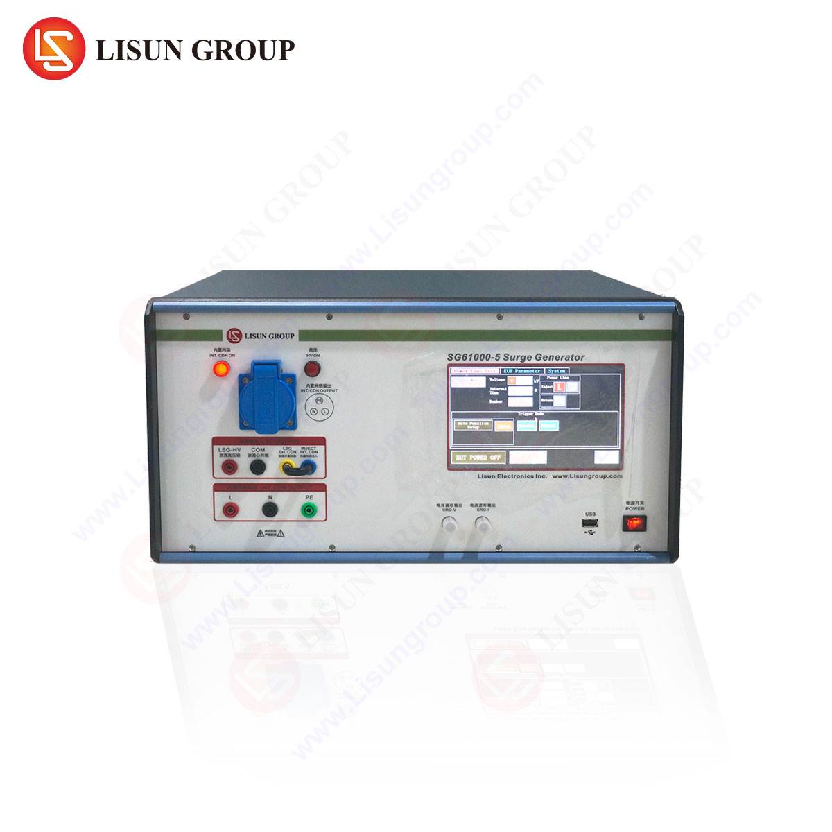
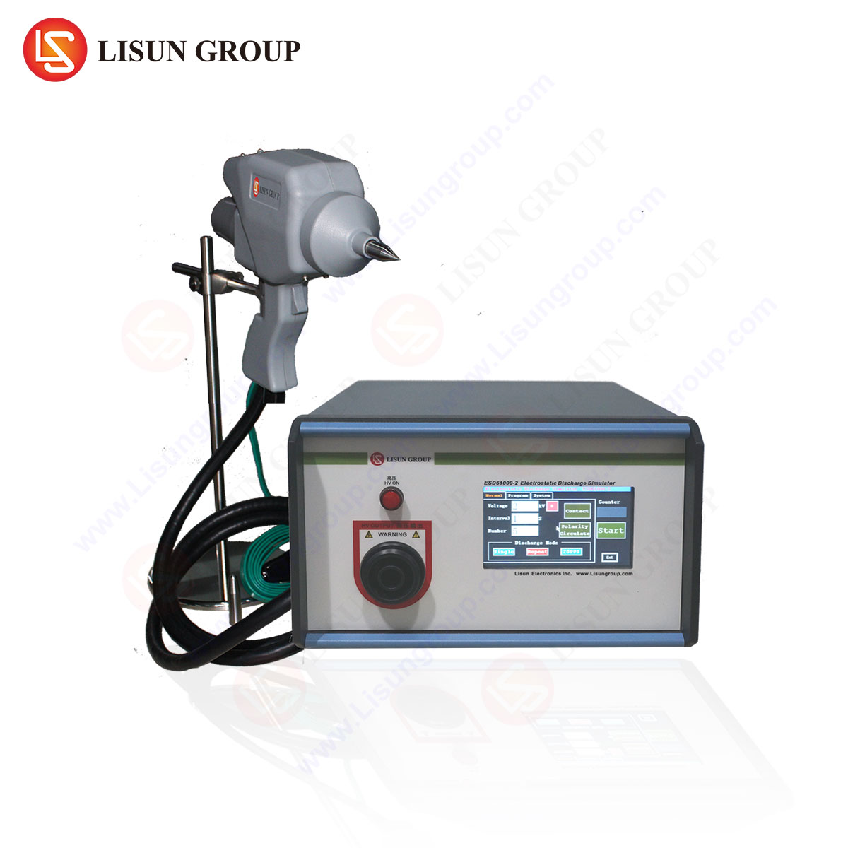
The integrity of any ESD qualification program rests upon the metrological precision of the discharge pulse. The LISUN ESD61000-2 series represents a class of contact-discharge simulators that integrate high-voltage power supplies, high-voltage relays, and pulse-forming networks within a single enclosure. The fundamental component is the 330 Ω / 150 pF discharge network, which is specified by the standard. However, the practical implementation of this network is critical. Stray inductance in the discharge path must be minimized to achieve the required current rise time of 0.7 to 1 ns.
The ESD61000-2C variant offers selectable contact and air discharge modes with voltage outputs up to ±30 kV. In a testing scenario for household appliances that feature capacitive touch interfaces, the air discharge mode introduces a non-deterministic element, as the approaching speed of the discharge electrode influences the breakdown voltage and thus the injected current spectral density. Conversely, the contact discharge mode, which the standard mandates for reproducibility, presents a deterministic waveform characterized by a peak current (I_p) of up to 30 A (at 8 kV) for a 2 kV setting. The LISUN generator utilizes a vacuum relay to switch between the storage capacitor and the discharge tip, mitigating the risk of pre-discharge or contact bounce. For the IC test engineer, the simulator’s built-in discharge counter and polarity switching capabilities facilitate extended stress tests, enabling the evaluation of cumulative degradation—a phenomenon where a device passes a single pulse but exhibits leakage current increase after 1,000 pulses.
Test Setup Topographies: Ground Planes, Coupling Planes, and Indirect Discharge
A persistent source of error in ESD testing is the physical layout of the test fixture, specifically the coupling to the ground reference plane (GRP). The IEC standard mandates a 1.6 mm thick aluminum GRP, but the connection of the Equipment Under Test (EUT) to this plane dictates the failure signature. For Industrial Equipment and Power Tools, which feature conductive housing, the discharge current may flow directly to the chassis ground; however, for Information Technology Equipment with plastic enclosures, the discharge occurs via parasitic capacitance to the GRP.
The LISUN ESD61000-2C facilitates vertical and horizontal coupling plane (VCP/HCP) testing, which is mandatory for IC qualification in Lighting Fixtures and Audio-Video Equipment. In VCP testing, the discharge is applied to a coupling plane that is parallel to the EUT, inducing a transient electromagnetic field rather than a direct current injection. This is a rigorous assessment of the IC’s immunity to radiated ESD fields, often revealing vulnerabilities in internal clock lines or reset circuitry rather than the power pins. The structural design of the ESD61000-2 series ensures that the discharge tip’s return cable is positioned perpendicular to the GRP to minimize loop area, which is essential for decreasing the induced magnetic field that can disturb high-impedance nodes in precision analog circuits used in Instrumentation. The varying discharge networks inside the generator—specifically the 150 pF storage capacitance—are calibrated against a Tektronix current target to ensure compliance with the ±10% tolerance on the peak current.
Discharge Waveform Analysis and the Secondary Current Pulse
The IEC 61000-4-2 waveform is broken into two distinct phases. The first phase, characterized by a 1 ns rise time and 4- to 5-ns duration at 30% of peak, is the constant current phase. The second phase, the decaying oscillatory phase, has a duration of approximately 30 ns for a total current of 15 A at 6 kV. For semiconductors, this secondary hump is the dominating cause of thermal stress. The energy deposited during this phase, calculated as the integral of i(t)^2 * R_dynamic, can raise the junction temperature of a small-area protection diode beyond the silicon’s intrinsic temperature, leading to filamentation and metallization melt.
Through the utilization of the LISUN ESD-883D, which incorporates a sophisticated high-voltage solid-state switch instead of traditional spark gaps, the waveform fidelity is maintained. The spark gap approach, historically used in older simulators, suffers from pulse-to-pulse amplitude jitter due to plasma formation fluctuations. The ESD-883D’s solid-state topology provides an autoregressive discharge with a repeatability of better than ±2%. This is paramount for Medical Devices, where IC qualification mandates a statistical confidence interval; a ±2% delta in peak current can be the deciding factor between a product entering clinical trials or failing biocompatibility interface validation.
Failure Mode Analysis: Latent Defects vs. Catastrophic Breakdown in ICs
When an ESD pulse is applied to a system, the IC may exhibit one of three responses: immunity (no effect), parametric deviation (temporary failure), or catastrophic breakdown (permanent damage). However, the most insidious is the latent defect. This is defined as a photomask-level damage that does not critically alter the functionality immediately but reduces the mean-time-to-failure (MTTF) due to electromigration or oxide trap-up.
For Automobile Industry applications, where components are subjected to variable climatic conditions and vibration, a latent defect is a harbinger of recall. Using the ESD61000-2C at elevated voltage levels (up to 15 kV air discharge) is a contractual requirement for many automotive OEMs. The discharge pulse’s high di/dt can generate a ground bounce of tens of volts within the IC package, potentially forward-biasing the parasitic diode between the p-substrate and the n-well. This injection of minority carriers can trigger a latch-up condition. During a latch-up, the current is limited only by the external circuit, effectively destroying the IC. Robust testing involves not just a single positive or negative pulse but a sequence of 10 positive and 10 negative pulses with a 1-second interval, a capability that the LISUN ESD61000-2 series provides through its automated polarity changeover.
Addressing ESD Performance in Harsh Operating Environments: Rail Transits and Spacecraft
In Rail Transit and Spacecraft, the ESD environment is not merely a human-generated event but often involves triboelectric charging from friction (e.g., wheels on rails, or satellite dielectric surfaces in low-earth orbit). Here, the discharge characteristics differ from the IEC 61000-4-2 standard model, exhibiting lower peak currents but significantly higher transferred charge. While the IEC model is the baseline, the compliance process often requires high-voltage margin testing. The LISUN ESD-883D, with its 30 kV maximum output, allows test engineers to exceed the standard’s Level 4 requirements to validate the external protection circuit’s extreme breakdown tolerance.
The circuit design for these environments often involves a transient voltage suppressor (TVS) external to the IC. The ESD generator’s output resistance (330 Ω) is significantly higher than the TVS’s dynamic resistance (< 1 Ω). Thus, the voltage clamp point at the IC pin is defined not by the generator’s voltage but by the TVS clamping voltage plus the IR drop across the PCB traces. The inductance of the PCB trace (typically 1 nH/mm) can cause a voltage spike of V = L di/dt. With a di/dt of 30 A/ns, a mere 3 nH of trace inductance yields 90 V of additional voltage drop. The LISUN simulator, when used in conjunction with a current clamp, allows engineers to measure this effective stress voltage at the IC pin, providing insights into the necessary PCB layout for Communication Transmission equipment where signal integrity is as important as ESD survivability.
Testing Protocols for Intelligent Equipment and Communication Transmission Modules
Intelligent equipment—such as IoT nodes and smart sensors—often incorporates high-speed digital buses (e.g., USB, HDMI, or Ethernet). These buses are particularly vulnerable to ESD due to the tight noise margins and high input impedance of the receiving ICs. The ESD immunity test for these devices requires direct discharges to the connector shell and indirect discharges to the surrounding coupling planes to simulate user interaction.
The LISUN ESD61000-2C includes a specialized discharge tip for testing unterminated connector pins, ensuring that the air discharge arc length is minimized. This is critical; an arc to a sharp metal corner of a USB connector will transition through a high-voltage, low-current arc phase before the main discharge, altering the spectral content. The contact discharge, preferred for its repeatability, is used for the inner pins. The simulator triggers an oscilloscope via a pre-trigger output, enabling time-correlated analysis of the IC’s data line response. In high-speed communication, the captured waveform can be compared against the eye diagram to characterize bit error rate (BER) degradation during ESD stress, a technique widely implemented in the evaluation of Communication Transmission equipment.
Thermal Management and Calibration Drift in ESD Generators
Ensuring the reliability of the ESD generator itself is crucial for long-term test accuracy. High-voltage operation generates internal heat within the charging resistor and the storage capacitor. The dielectric absorption of the capacitor can alter the effective capacitance value with temperature, leading to a longer RC decay time constant and a malformed secondary pulse. The LISUN ESD-883D addresses this using polypropylene film capacitors, which exhibit low dielectric absorption coefficient and a high insulation resistance, ensuring stable discharge characteristics over a wide range of ambient temperatures (0°C to 40°C).
Calibration drift is a common issue in high-voltage instrumentation. The internal voltage meter in many low-cost simulators relies on resistor dividers that have a high temperature coefficient. In the ESD61000-2 series, the voltage divider utilizes thick film surface-mount resistors with a temperature coefficient of ±25 ppm, providing a voltage set-point accuracy of +5% as mandated by the standard. The current waveform is calibrated using a target that conforms to the geometry specified in the standard; the calibration is conducted using a 2 GHz bandwidth oscilloscope to accurately capture the 1 ns rise time without bandwidth attenuation artifacts. This level of metrology is essential for R&D laboratories that wish to audit their test equipment according to ISO 17025 standards.
Comparative Advantages of the LISUN ESD61000-2 Series and ESD-883D in the Testing Arsenal
Distinguishing between the models within the LISUN lineup is based on the application complexity and the voltage requirements. The ESD61000-2 (base model) provides the essential 30 kV capability with contact and air discharge modes, suitable for production line sampling of Low-voltage Electrical Appliances and Electronic Components. The ESD61000-2C adds an RS232 interface and PC-control software for detailed test report generation, a necessity for the audit trails required in the Power Equipment sector.
The ESD-883D stands as the pinnacle of the series. It implements a dual-channel discharge system that can meet the specific test requirements for higher-level compliance, such as the automotive EMC directive 2004/104/EC. Its unique feature is the capability to adjust the pulse repetition frequency, which allows for burst testing at 20 pulses per second. This is crucial for detecting intermittent failures in systems with dynamic power management. In contrast, the standard requires at least 1 second between discharges; however, for detecting soft errors in space-grade devices, a high repetition rate is necessary to cumulatively charge the substrate without giving the device time to recover. The ESD-883D’s ultra-low EMI design ensures that the control electronics are not disturbed by the high voltage discharge, maintaining stability in the output over extended burn-in tests.
The Role of ESD Testing in Product Certification for Medical and Low-Voltage Appliances
Medical devices classified as life-supporting or life-sustaining fall under stringent regulatory scrutiny. The IEC 61000-4-2 test is a mandatory portion of the IEC 60601-1-2 electromagnetic compatibility standard. Here, the ESD test must be performed not only at the enclosure but also on any metallic parts that a patient might touch. The LISUN ESD61000-2 series is configured with interchangeable discharge tips—including the standard pointed tip and the hemispheric tip—to comply with the specific requirements for skin-contact discharges. The failure criterion for Medical Devices is often no deviation in the physiological monitoring waveform. This requires the test engineer to use reduced discharge voltages initially to perform a sensitivity analysis, mapping out which specific discharge locations lead to a transient on the ECG output. The simulator’s precise charge metering allows for this incremental voltage step testing (e.g., ±500 V increments) up to a failure threshold, which is a protocol seldom discussed in generic literature but is a best practice for isolating sensitive analog front ends in instrumentation.
Best Practices for Designing an ESD Test Plan for IC and System Validation
A comprehensive ESD test plan should encompass more than just the required levels of the standard. It should include direct contact discharges to all accessible conductive surfaces, indirect discharges to the HCP and VCP, and air discharges to metallic coated plastics. The plan should also specify the number of discharges (typically 10 positive, 10 negative at each test point) and the polarity switching sequence. For IC protection verification, the test plan must include a functional test after each pulse. The LISUN ESD61000-2C’s software can automatically integrate with the functional test instrumentation via a GPIB/IEEE-488 interface, creating a closed-loop system that pauses the ESD sequence upon detecting a functional failure, thus logging the exact number of pulses to failure. This statistical approach is invaluable for Spacecraft applications where the component count is high and the cost of failure is astronomical.
Future Trends in ESD Simulation: Transient Interference and Sensor Networks
The future of ESD testing is trending toward multi-source interference, where system-level ESD occurring at one point induces coupled transients elsewhere. The hard switching of high-voltage circuit breakers in Power Equipment can generate a damped oscillatory transient (ring wave) that is distinct from the IEC 61000-4-2 waveform. While the standard addresses this separately (IEC 61000-4-12), the latest research suggests that ICs have different failure thresholds for ring waves versus the unidirectional ESD pulse. The next generation of simulators, exemplified by the modular RFI approach in the ESD-883D, aims to combine these waveforms. For now, mastering the basic ESD pulse remains the cornerstone of semiconductor protection. Through meticulous attention to the discharge path, comprehension of waveform physics, and utilization of a precision simulator such as the LISUN ESD61000-2 series, reliability engineers can significantly enhance the robustness of electronic systems across all the afore-mentioned sectors, from Low-voltage Electrical Appliances to advanced Automobile Industry telematics modules.
Frequently Asked Questions (FAQ)
Q1: Why does the LISUN ESD61000-2 series specify a 330 Ω resistor? Can that be changed for testing high-power electronics?
A: The 330 Ω resistor is the human body equivalent resistance defined by IEC 61000-4-2. It dictates the peak current for a given voltage. Modifying it would invalidate the test according to the standard. For high-power electronics that require higher current for ESD simulation, the test setup should be expanded to include direct coupling to the housing, but the generator itself must remain compliant to the specified network.
Q2: What is the practical difference between the ESD61000-2C and the ESD-883D when testing medical devices?
A: The ESD-883D offers higher pulse repetition rates and a more advanced solid-state switching time, facilitating accelerated stress tests (AST) that simulate years of patient interaction in a few hours. The ESD61000-2C is sufficient for standard type approval tests (single pulse with 1-second intervals). The choice depends on whether your R&D requires burn-in at high repetition rates to find maximum degradation levels.
Q3: How do I calibrate my LISUN simulator in accordance with IEC 61000-4-2 to ensure the secondary pulse is correct?
A: Calibration occurs via a standard current target (manufactured by LISUN) placed in the discharge path. You must discharge the gun into the target and observe the resultant current on a 1 GHz or higher bandwidth oscilloscope. You are checking for T1 (rise time) between 0.6 and 1 ns and T2 (duration) at 30% peak between 25 and 30 ns. A calibration interval of 12 months is recommended.
Q4: Is air discharge or contact discharge the “harder” test for integrated circuit immunity?
A: Generally, contact discharge is considered more reproducible, while air discharge can induce a higher-frequency spectral component due to the rapid ionization of the air gap. Air discharge tends to be more severe for devices with large parasitic capacitance, as the voltage is not clamped until the air breaks down. Many IC failures are observed only under air discharge due to the pre-pulse a few nanoseconds before the main surge. It is recommended to perform both.
Q5: Can a standard ESD gun test damage the IC directly even if the circuit is inside a plastic enclosure?
A: Yes. The discharge applied to the plastic enclosure creates a large electromagnetic field that induces a voltage into the internal signal traces. This induced transient can couple to the IC’s VCC and GND pins, causing a supply voltage spike or latch-up. The LISUN ESD61000-2 series supports VCP/HCP testing to simulate this indirect coupling, which is essential for plastic-cased consumer products.