Fundamentals of Electrostatic Discharge and Its Impact on Electronic Systems
The proliferation of sophisticated electronics across diverse industrial sectors has rendered the management of electrostatic discharge (ESD) a critical discipline. ESD, the sudden flow of electricity between two electrically charged objects, represents a pervasive and insidious threat to the integrity and reliability of electronic components and systems. While human-body model (HBM) ESD events are a primary concern, the Charged Device Model (CDM) has emerged as a dominant failure mechanism in automated manufacturing environments. CDM events occur when a component itself becomes triboelectrically charged and then rapidly discharges to a conductive surface or ground. These discharges are characterized by extremely fast rise times and high peak currents, capable of causing latent damage, gate oxide ruptures, and catastrophic failures in integrated circuits (ICs). Mitigating CDM risks necessitates specialized test equipment capable of accurately simulating these real-world events under controlled laboratory conditions.
The Critical Role of Charged Device Model Simulation in Quality Assurance
As electronic components become smaller, faster, and more complex, their inherent susceptibility to CDM ESD increases. The transition to finer semiconductor process geometries, such as those below 10nm, has resulted in thinner gate oxides and reduced spacing between interconnects, lowering the energy threshold required for ESD-induced damage. A CDM event, while often containing less total energy than an HBM event, delivers its energy over a much shorter duration, typically a few nanoseconds. This results in current pulses that can exceed 10 Amperes, posing a severe threat to sensitive structures within a chip. Consequently, comprehensive CDM testing is no longer an optional quality check but a mandatory step in the product qualification lifecycle for manufacturers of high-reliability electronics. It is integral to failure analysis, process control verification, and ultimately, ensuring the field reliability of the final product.
Architectural Overview of the LISUN ESD-CDM Test System
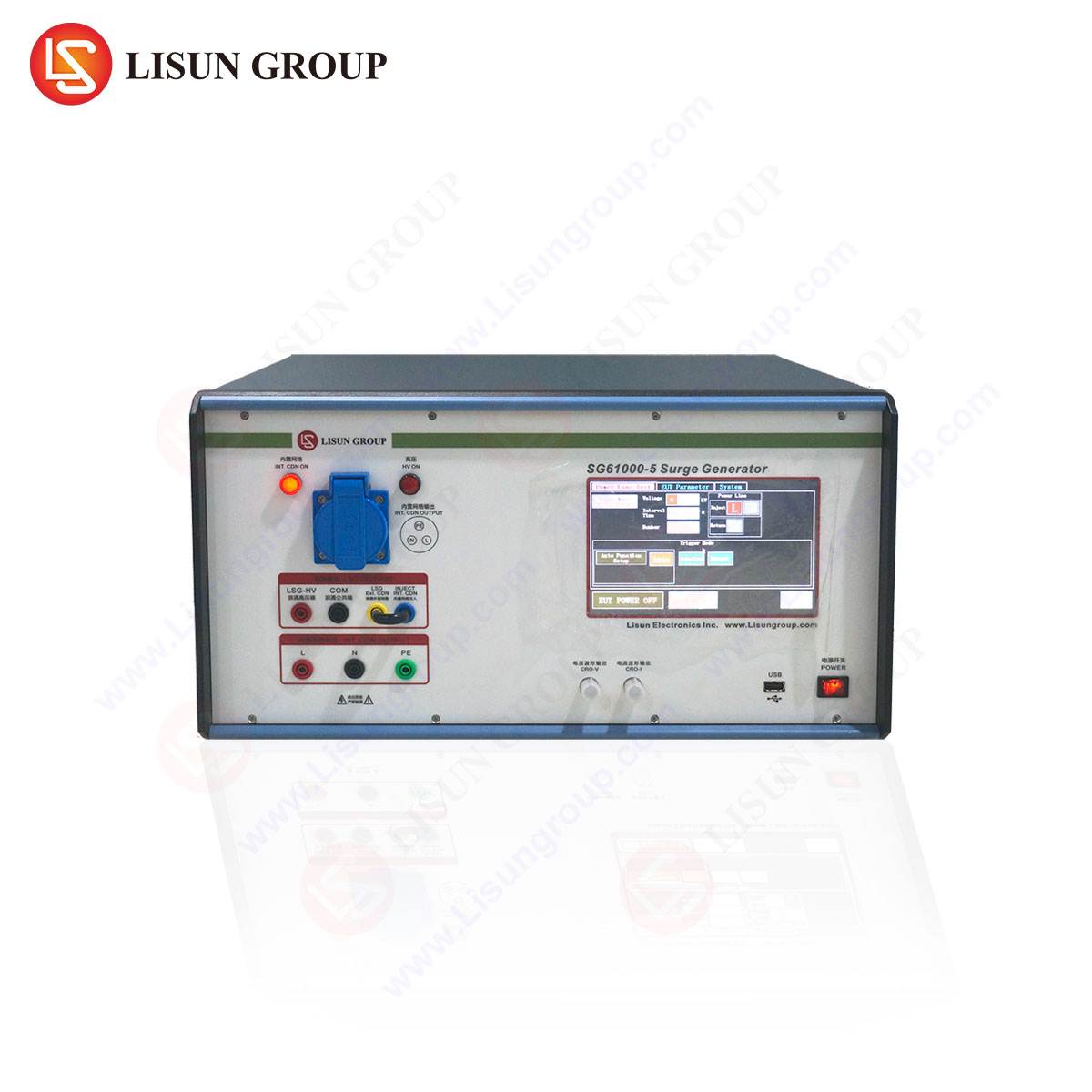
The LISUN ESD-CDM test system is engineered to provide a precise and repeatable platform for simulating CDM ESD events in compliance with major international standards, including ANSI/ESDA/JEDEC JS-002 and IEC 61000-4-2. The system’s architecture is predicated on delivering a waveform that faithfully replicates the physical phenomena of a charged device discharge. Its core components include a high-voltage DC power supply for charging the device under test (DUT), a high-speed relay for initiating the discharge, a calibrated current sensor, and a dedicated field plate that serves as the discharge target. The system is controlled via an intuitive software interface that allows for the programming of test parameters, sequencing, and real-time monitoring of discharge waveforms. The mechanical design incorporates a shielded enclosure to minimize electromagnetic interference (EMI) and ensure the integrity of the test results, while a robotic or manual positioning system ensures consistent and accurate discharge point application.
Analyzing the Key Specifications and Performance Metrics
The performance of a CDM simulator is defined by a set of critical specifications that govern its accuracy and reliability. The LISUN ESD-CDM system is characterized by the following parameters:
- Discharge Voltage Range: Typically programmable from 125V to ±2000V, covering the full spectrum of test conditions required by contemporary standards for components ranging from consumer-grade to automotive-grade.
- Rise Time: The system achieves a rise time of less than 500 picoseconds, which is crucial for accurately simulating the ultra-fast nature of a real CDM event. This parameter is directly verified against the requirements of the target standards.
- Peak Current: At a 500V discharge level, the peak current exceeds 5 Amperes, with the current amplitude scaling linearly with the charging voltage. This high-current capability is essential for stressing the DUT’s internal protection structures.
- Waveform Verification: The system includes integrated waveform verification tools to ensure that the generated current pulse conforms to the specified waveform parameters, such as peak current (Ip), rise time (tr), and current at specific time intervals (I1, I2), as defined by the standard’s template.
Table 1: Representative LISUN ESD-CDM Specifications
| Parameter | Specification | Compliance Standard |
| :— | :— | :— |
| Discharge Voltage Range | ±125V to ±2000V | ANSI/ESDA/JEDEC JS-002 |
| Rise Time (tr) | 5 A | ANSI/ESDA/JEDEC JS-002 |
| Discharge Resistor | 1 Ω (nominal) | ANSI/ESDA/JEDEC JS-002 |
| Relay Type | High-Speed, Low-Bounce | N/A |
| Control Interface | PC Software & Touch Panel | N/A |
Operational Methodology and Testing Protocol
The testing protocol with the LISUN ESD-CDM system follows a rigorous, standards-based methodology. The process begins with the proper mounting of the DUT onto the field plate, which is connected to the ground plane. The DUT is oriented with its pins facing upwards. The system’s pogo pin, connected to the discharge head, is then positioned to contact a specific pin of the DUT. The test sequence involves charging the DUT’s body capacitance to a predefined voltage level. Once charged, the high-speed relay is triggered, creating a low-impedance path from the DUT to the ground plane through the pogo pin. The resultant discharge current flows through the current sensor, and the waveform is captured by a high-bandwidth oscilloscope. This process is repeated for all relevant pin combinations (e.g., pin-to-all-other-pins) and at progressively increasing voltage levels until the failure threshold of the device is determined. The system software automates this entire process, logging all discharge events and corresponding DUT performance data for post-test analysis.
Sector-Specific Applications and Compliance Imperatives
The application of CDM testing spans virtually all industries that incorporate modern electronics. The LISUN ESD-CDM system is deployed to ensure product robustness in the following sectors:
- Automotive Industry: Electronic Control Units (ECUs), sensors, and infotainment systems are subjected to harsh electrical environments. CDM testing is mandated by standards such as AEC-Q100 to prevent latent failures that could lead to safety-critical system malfunctions.
- Medical Devices: Pacemakers, insulin pumps, and diagnostic imaging equipment demand the highest levels of reliability. A CDM-induced failure in a medical IC could have dire consequences, making comprehensive ESD qualification non-negotiable.
- Communication Transmission and Information Technology Equipment: Network routers, servers, and base station components handle high-speed data. CDM robustness is essential to maintain data integrity and system uptime.
- Aerospace and Rail Transit: Avionics and train control systems operate in environments with significant static charge buildup. The failure of a single component due to a CDM event can compromise the entire vehicle system.
- Household Appliances and Intelligent Equipment: As appliances become “smarter” with more embedded electronics, ensuring their resilience against ESD during handling and assembly is key to reducing warranty returns and improving brand reputation.
- Electronic Components and Instrumentation: Semiconductor manufacturers and their customers use CDM testers for device qualification, process monitoring, and comparative analysis of different component lots.
Comparative Analysis with Alternative ESD Testing Methodologies
It is imperative to distinguish CDM testing from other ESD models. The Human-Body Model (HBM) simulates a person discharging static electricity through a device, featuring a slower rise time (2-10 ns) and a longer duration (~150 ns) pulse. The Machine Model (MM), derived from a Japanese standard, simulates a discharge from a charged machine and is characterized by a near-zero impedance, producing a high-energy oscillatory current pulse. In contrast, the CDM pulse is the fastest, with a sub-nanosecond rise time and a total duration of less than 5 nanoseconds. This fundamental difference in the discharge characteristics means that a device that passes HBM testing may still be highly vulnerable to CDM events. Therefore, a comprehensive ESD control strategy must include dedicated testing for both HBM and CDM failure mechanisms.
Advancements in Test Automation and Data Integrity
Modern ESD test systems, like the LISUN ESD-CDM, have evolved beyond simple pulse generators into sophisticated data acquisition and analysis platforms. Key advancements include full automation of the test sequence, which eliminates operator-induced variability and enhances repeatability. Integrated software not only controls the voltage levels and pin sequencing but also interfaces with parametric testers to perform pre- and post-stress functional tests on the DUT. This allows for the precise identification of failure thresholds and the nature of the degradation. Furthermore, these systems feature comprehensive data logging, storing every discharge waveform alongside the corresponding DUT response. This creates an auditable trail for quality assurance and provides invaluable data for root-cause analysis in the event of a failure, enabling continuous improvement in both component design and manufacturing processes.
Frequently Asked Questions (FAQ)
Q1: What is the primary physical difference between a Human-Body Model (HBM) and a Charged Device Model (CDM) ESD event?
A1: The primary difference lies in the source of the charge and the discharge path. An HBM event originates from a charged human body and discharges through the device. A CDM event originates from the device itself becoming charged, and it discharges its stored energy to a grounded conductor. This results in a much faster, higher-current pulse for CDM compared to HBM.
Q2: Why is the rise time of the CDM pulse so critical, and how is it verified?
A2: The sub-nanosecond rise time is critical because it determines the frequency content of the pulse and how the current is distributed within the integrated circuit. Faster rise times can bypass on-chip protection circuits designed for slower HBM events, leading to internal damage. Verification is performed using a calibrated current target and a high-bandwidth oscilloscope (typically > 4 GHz) to ensure the measured waveform falls within the parameters defined by the applicable standard (e.g., JS-002).
Q3: In an automated production environment, what are the most common sources of CDM events?
A3: Common sources include automated handling equipment, conveyor belts, vacuum pick-and-place nozzles, and non-conductive trays or tubes. Any process where a device moves or slides against a material can triboelectrically charge the device, setting the stage for a rapid discharge when it subsequently contacts a metallic surface, such as a test socket or a PCB.
Q4: Can the LISUN ESD-CDM system be used to test fully assembled printed circuit boards (PCBs)?
A4: The standard CDM test methodology is designed for individual, unpackaged or packaged semiconductor devices. Testing assembled PCBs introduces significant parasitic capacitance and inductance, which alter the discharge waveform and make results non-compliant with component-level CDM standards. For board-level ESD assessment, the system-level ESD test per IEC 61000-4-2, typically performed using an ESD gun, is the appropriate methodology.
Q5: How does the calibration of the CDM test system ensure long-term measurement accuracy?
A5: The system’s calibration involves using a certified current target and a traceable oscilloscope to measure the generated waveform. This process verifies that key parameters like peak current, rise time, and full-width at half-maximum (FWHM) are within the specified tolerances. Regular calibration, typically on an annual basis, is essential to correct for any drift in the system’s components and to maintain the integrity and reproducibility of all test data.


