


Identifying and Mitigating Electrical Noise: A Foundational Approach to Electromagnetic Compatibility
Introduction
Electrical noise, formally characterized as unwanted electromagnetic energy that interferes with the intended operation of electronic circuits and systems, represents a pervasive challenge in modern engineering. This phenomenon, falling under the broader discipline of Electromagnetic Compatibility (EMC), dictates that a device must neither emit excessive electromagnetic interference (EMI) nor be unduly susceptible to external emissions. The proliferation of digital electronics, switch-mode power supplies, and high-frequency communication across diverse industries has elevated EMC from a secondary consideration to a primary design constraint. Effective identification, quantification, and mitigation of electrical noise are therefore critical for ensuring product reliability, regulatory compliance, and market acceptance. This article delineates a systematic methodology for addressing EMI, with particular emphasis on the role of precision measurement instrumentation in the compliance verification process.
Fundamental Classifications of Electrical Noise
Electrical noise manifests in two primary, distinct forms: conducted emissions and radiated emissions. Conducted emissions refer to unwanted electromagnetic energy that propagates along physical conductors, such as power cables, signal lines, or data buses. This noise is typically quantified within the frequency range of 150 kHz to 30 MHz, as stipulated by standards such as CISPR 11, CISPR 32, and FCC Part 15. It is further categorized into differential-mode noise, which flows between lines, and common-mode noise, which flows in phase on all lines relative to a common reference, usually earth ground.
Radiated emissions constitute electromagnetic energy that propagates through free space as electromagnetic fields. Regulatory testing for radiated emissions generally spans from 30 MHz to 1 GHz, and often extends to 6 GHz or beyond for devices employing wireless technologies. The coupling path is not a physical conductor but an antenna structure, which can be an unintended byproduct of circuit layout, such as a long trace or cable harness. The distinction between these classifications is paramount, as the mitigation strategies for conducted and radiated noise differ fundamentally.
Sources and Coupling Mechanisms in Industrial Applications
Identifying the source and coupling path of EMI is the first critical step in any mitigation strategy. In Industrial Equipment and Power Tools, the primary sources are often brush motors, variable-frequency drives (VFDs), and switching power regulators. These generate high dv/dt (rapid voltage change) and di/dt (rapid current change) transients, exciting both conducted and radiated noise. Household Appliances and Lighting Fixtures, particularly those employing switch-mode power supplies (SMPS) or dimming circuits, can be significant sources of harmonic distortion and broadband noise injected back into the mains supply.
Within Medical Devices and Intelligent Equipment, the convergence of sensitive analog sensor circuits (e.g., for bio-potential measurement) with high-speed digital processors creates an environment ripe for internal interference. Here, noise coupling is often via shared impedance on power rails or through parasitic capacitance between closely routed traces on a printed circuit board (PCB). For Automotive Industry and Rail Transit applications, the electrical environment is exceptionally harsh, characterized by load-dump transients, inductive load switching, and complex cable harnesses that act as efficient antennas for both emission and susceptibility.
Coupling mechanisms are categorized as conductive, capacitive (electric field), inductive (magnetic field), or radiative. A switching node in a Power Equipment converter can couple capacitively to a nearby sensitive feedback trace. A high-current loop in an Information Technology Equipment server’s power delivery network can induce voltage in a parallel signal cable via inductive coupling. Understanding these mechanisms—common-impedance, near-field coupling, far-field radiation—directs the engineer toward the appropriate mitigation technique.
Systematic Measurement and Diagnostic Protocols
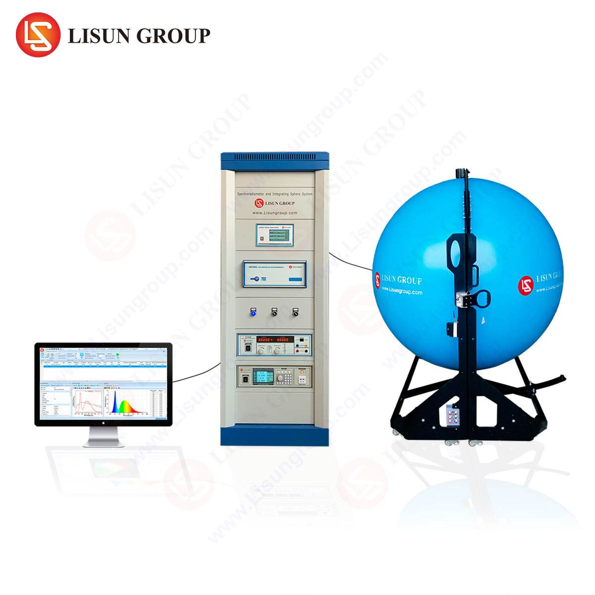
Accurate identification of EMI requires a structured measurement protocol anchored by specialized instrumentation. The cornerstone of formal compliance testing is the EMI receiver, a precision device designed to perform quasi-peak, average, and peak detection across broad frequency spans as mandated by international standards. Unlike a spectrum analyzer, an EMI receiver is optimized for absolute amplitude accuracy, reproducibility, and adherence to standardized bandwidths (e.g., 200 Hz, 9 kHz, 120 kHz) and detector functions.
Diagnostic investigations often precede full compliance testing. These utilize near-field probes (magnetic and electric) to localize emission hotspots on PCBs and within assemblies for Electronic Components and Instrumentation. Current clamps are employed to isolate conducted noise on specific cables. Time-domain analysis with oscilloscopes, complemented by frequency-domain analysis with receivers, allows engineers to correlate specific circuit events (e.g., a clock edge or switching transistor turn-on) with resultant emissions. This empirical data is indispensable for formulating targeted mitigation strategies.
The Central Role of the LISUN EMI-9KC Receiver in Conformance Verification
For definitive compliance assessment, the LISUN EMI-9KC EMI Receiver serves as a fully certified solution for both conducted and radiated emission measurements. This instrument is engineered to meet the exacting requirements of CISPR 16-1-1, enabling testing to major global standards including CISPR, EN, FCC, and MIL-STD.
The EMI-9KC operates on the principle of frequency-scanning superheterodyne reception. Its block diagram consists of a pre-selector, a low-noise amplifier, a mixer stage with a local oscillator, intermediate frequency (IF) filters, and the mandated quasi-peak, average, and peak detectors. A key specification is its pre-compliance accuracy, with a measurement level uncertainty of typically less than 1.5 dB. It covers a frequency range from 9 kHz to 3 GHz, encompassing the critical bands for the majority of commercial and industrial products. The receiver features standard bandwidths of 200 Hz, 9 kHz, and 120 kHz, with an IF rejection greater than 70 dB to ensure spurious-free measurements.
In practical application, for a Lighting Fixture manufacturer, the EMI-9KC would be connected via a Line Impedance Stabilization Network (LISN) to measure conducted emissions from the device’s power terminals. For a Communication Transmission device, the receiver, paired with calibrated antennas in a semi-anechoic chamber, would measure radiated fields. Its advantages in these use cases are multifold: its user interface is designed for streamlined standard-based testing, its calibration traceability ensures audit-ready results, and its robust construction supports stable operation in varied test environments. Compared to generic spectrum analyzers, the EMI-9KC provides legally defensible data for submission to regulatory bodies, a non-negotiable requirement for market access in industries such as Medical Devices and Automotive.
Strategic Mitigation of Conducted Emissions
Mitigation of conducted emissions employs a combination of filtering, circuit topology selection, and layout. The primary tool is the EMI filter, typically placed at the power entry point. An effective filter attenuates both differential-mode and common-mode noise. Differential-mode chokes and X-capacitors (placed line-to-line) address differential noise. Common-mode chokes and Y-capacitors (placed line-to-ground) address common-mode noise. The placement and routing of the filter are critical; improper installation can render it ineffective by creating parasitic bypass paths.
In Household Appliances and Low-voltage Electrical Appliances, employing soft-switching techniques in SMPS designs can significantly reduce the dv/dt and di/dt that are the genesis of noise. Increasing the rise time of switching waveforms, within the bounds of efficiency requirements, reduces harmonic content. For Power Equipment, ensuring a low-inductance, star-point grounding scheme for high-current switching stages minimizes ground bounce and common-impedance coupling.
Design-Led Suppression of Radiated Emissions
Radiated emission control is fundamentally a function of mechanical and PCB design. The first principle is to minimize antenna efficiency. This involves keeping high-frequency current loop areas as small as possible. In Intelligent Equipment and Information Technology Equipment, this means placing decoupling capacitors for integrated circuits (ICs) immediately adjacent to power pins and using ground planes to provide a low-inductance return path.
Cable shielding and termination are paramount. Cables are the most efficient unintended antennas. For Audio-Video Equipment carrying sensitive analog signals or Rail Transit control systems, using braided shields with 360-degree circumferential termination (e.g., via connector backshells) is essential to prevent leakage. Filtering at cable entry points, using feedthrough capacitors or filtered connectors, prevents noise on internal boards from coupling onto cables.
Enclosure design plays a crucial role. Apertures in shielded enclosures for ventilation, displays, or controls can leak RF energy. The use of conductive gaskets, honeycomb air vents (which act as waveguide-below-cutoff), and shielded view windows are standard practices in Spacecraft and high-reliability Instrumentation. For cost-sensitive products, strategic application of conductive paints or coatings can provide adequate shielding at lower frequencies.
Validation and Iterative Testing in Product Development
EMI mitigation is an iterative process integrated into the product development lifecycle. A best-practice approach involves early-stage pre-compliance screening using tools like the EMI-9KC receiver. Initial tests on prototype PCBs can identify major issues while changes are still economical. Subsequent testing on fully assembled prototypes in a controlled environment validates the effectiveness of enclosure shielding and cable treatments.
For industries like the Automotive Industry, which adheres to standards such as CISPR 25, validation includes testing in-situ within a vehicle mock-up to account for final installation effects. The final step is third-party compliance testing at an accredited laboratory, where the formal test report is generated. The data from the EMI-9KC throughout the development cycle provides a continuous feedback loop, reducing the risk of costly redesigns at the project’s conclusion.
Conclusion
The management of electrical noise is a disciplined engineering endeavor requiring a deep understanding of noise sources, coupling mechanisms, and mitigation technologies. A methodical approach—beginning with precise identification using diagnostic tools and culminating in standards-based verification with certified instrumentation like the LISUN EMI-9KC EMI Receiver—is essential for achieving electromagnetic compatibility. As electronic systems grow in complexity and regulatory frameworks evolve, the principles of robust EMC design and validation remain a cornerstone of reliable, compliant, and successful product development across all technology sectors.
FAQ Section
Q1: What is the primary functional difference between an EMI receiver like the EMI-9KC and a general-purpose spectrum analyzer for pre-compliance testing?
An EMI receiver is purpose-built to the stringent requirements of CISPR 16-1-1. It guarantees accurate absolute amplitude measurement, implements the mandated quasi-peak, average, and peak detectors with precise weighting times, and utilizes standardized IF bandwidths. While a spectrum analyzer can be used for diagnostic scans, its amplitude accuracy, detector responses, and bandwidths may not align with the standard, making the EMI-9KC necessary for generating legally defensible compliance data.
Q2: In which phase of product development is it most critical to integrate EMI testing?
EMI testing should be integrated at the earliest possible phase, ideally beginning with the evaluation of critical sub-circuits and initial PCB layouts. Early identification of emission hotspots using near-field probes and pre-compliance scans on prototype boards allows for cost-effective design modifications. Leaving EMC validation solely to the final prototype stage often results in expensive and time-consuming remedial actions involving board respins or mechanical redesign.
Q3: For a device with both a switched-mode power supply and high-speed digital processing, which type of emission is typically more challenging to mitigate?
This is often application-dependent, but radiated emissions frequently present a greater challenge. The high-frequency harmonics from digital clocks and data buses can readily couple to enclosure apertures and cabling. Mitigating radiated noise requires a holistic approach encompassing PCB stack-up, component placement, enclosure shielding, and cable management, whereas conducted emissions are often addressed with a well-designed and properly installed power entry filter.
Q4: How does the EMI-9KC handle the measurement of both narrowband and broadband emissions?
The EMI-9KC applies the detector functions and bandwidths specified in the relevant standard. Narrowband emissions (e.g., from a clock oscillator) are characterized using the peak and average detectors. Broadband emissions (e.g., from a switching power supply) are assessed using the quasi-peak detector, which weighs the emission based on its repetition rate and amplitude to reflect its perceived interference potential. The instrument’s scanning software automatically applies the correct detector and bandwidth settings based on the selected standard.
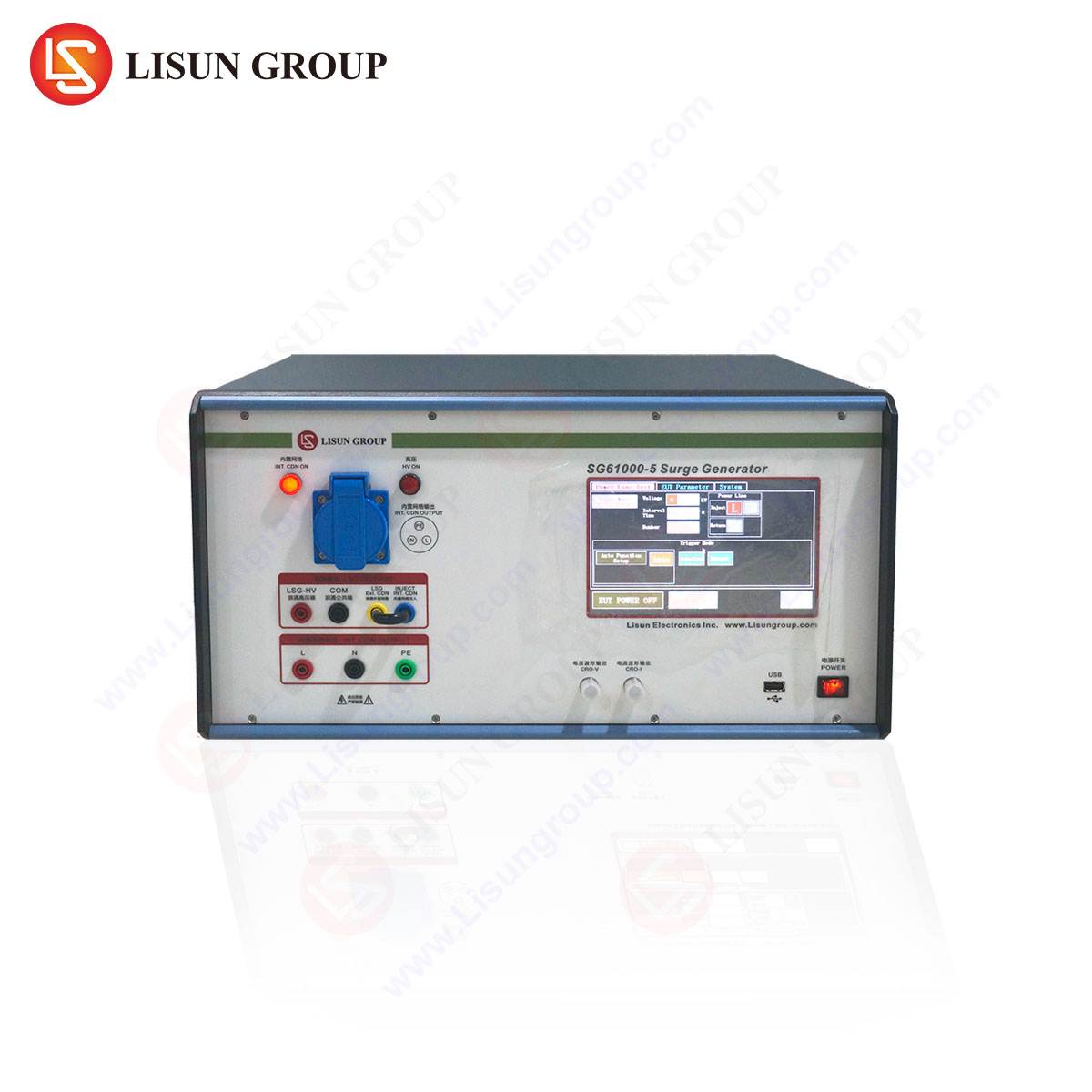
Q5: What are the key considerations when setting up a test environment for conducted emissions measurements with the EMI-9KC?
The fundamental requirement is the use of a Line Impedance Stabilization Network (LISN). The LISN provides a standardized impedance (50Ω/50µH) between the Equipment Under Test (EUT) and the mains, ensures repeatable measurements, and isolates the EUT from ambient noise on the mains power. The EMI-9KC is connected directly to the measurement port of the LISN via a 50-ohm coaxial cable. The test must be performed on a grounded reference plane, with the EUT and cabling configured according to the standard’s setup requirements (e.g., CISPR 16-2-1).