


Advancements in Electrostatic Discharge Simulation Analysis for Robust Product Design
Abstract
The increasing miniaturization of semiconductor geometries and the proliferation of sensitive electronic components across diverse industries have rendered electrostatic discharge (ESD) a primary cause of latent and catastrophic device failure. Traditional post-production ESD testing, while necessary for validation, is a reactive measure that can lead to costly design iterations and project delays. This article examines the critical role of ESD simulation analysis as a proactive, integrated design methodology. By leveraging advanced simulation tools, engineers can predict ESD susceptibility, optimize protection strategies, and achieve first-pass design success. The discussion is contextualized with the capabilities of the LISUN ESD61000-2 ESD Simulator, a state-of-the-art instrument for validating both component and system-level robustness against standardized ESD threats.
Fundamental Principles of Electrostatic Discharge Phenomena
Electrostatic discharge is a transient transfer of electric charge between two objects at different electrostatic potentials. This event, lasting nanoseconds to microseconds, can involve currents of several amperes and voltages in the kilovolt range. The damage mechanism is twofold: thermal and electromagnetic. Thermal damage results from the rapid joule heating at a semiconductor junction, causing localized melting and silicon ablation. Electromagnetic damage is caused by the intense, high-frequency electromagnetic fields (EMI) generated by the fast-rising current transient, which can induce parasitic voltages and currents in adjacent circuits, leading to latch-up or logic state corruption.
Two primary ESD event models are universally recognized. The Human Body Model (HBM) simulates the discharge from a charged human being through a series resistance to a device. The International Electrotechnical Commission (IEC) 61000-4-2 standard defines a system-level ESD test that models a human discharging through a handheld metallic object, such as a tool. This standard specifies a current waveform with a very fast rise time of 0.7 to 1 nanosecond and a peak current that must be achieved at various test voltages (e.g., 3.75A at 2kV, 7.5A at 4kV, 15A at 8kV). Accurate simulation and testing require equipment capable of faithfully replicating this stringent waveform.
Methodologies for ESD Simulation in Electronic Systems
ESD simulation analysis is a multi-physics endeavor, combining circuit simulation, electromagnetic field solving, and thermal analysis. The process typically involves several discrete but interconnected stages.
The initial stage involves creating a high-fidelity model of the ESD pulse itself. This is achieved using a piece-wise linear (PWL) voltage source or a dedicated ESD generator model, such as the one defined in the IEC 61000-4-2 standard, which includes the network of resistors and capacitors that shape the characteristic current waveform. The accuracy of this source model is paramount, as an incorrect waveform will invalidate all subsequent analysis.
Subsequently, a 3D model of the product under test is constructed. This model must include the chassis, printed circuit board (PCB), critical traces, and the integrated circuits (ICs) with their internal ESD protection structures. For industries like Automobile Industry and Rail Transit, where control units are housed in complex metallic enclosures, the geometry of the enclosure, seam apertures, and cable port placements become critical factors in determining the current discharge path and the resulting internal electromagnetic fields. Using a method such as the Finite-Difference Time-Domain (FDTD) or the Method of Moments (MoM), solvers calculate the propagation of the ESD current across the structure and the coupling of electromagnetic energy into nearby circuits.
The final stage integrates the extracted parasitic elements (resistance, inductance, capacitance) from the 3D EM analysis into a circuit simulator like SPICE. Here, the transient voltage and current stresses on individual IC pins are precisely calculated. This allows designers to verify whether the on-chip or board-level protection circuits will clamp the voltage to a safe level below the breakdown voltage of the protected core transistor.
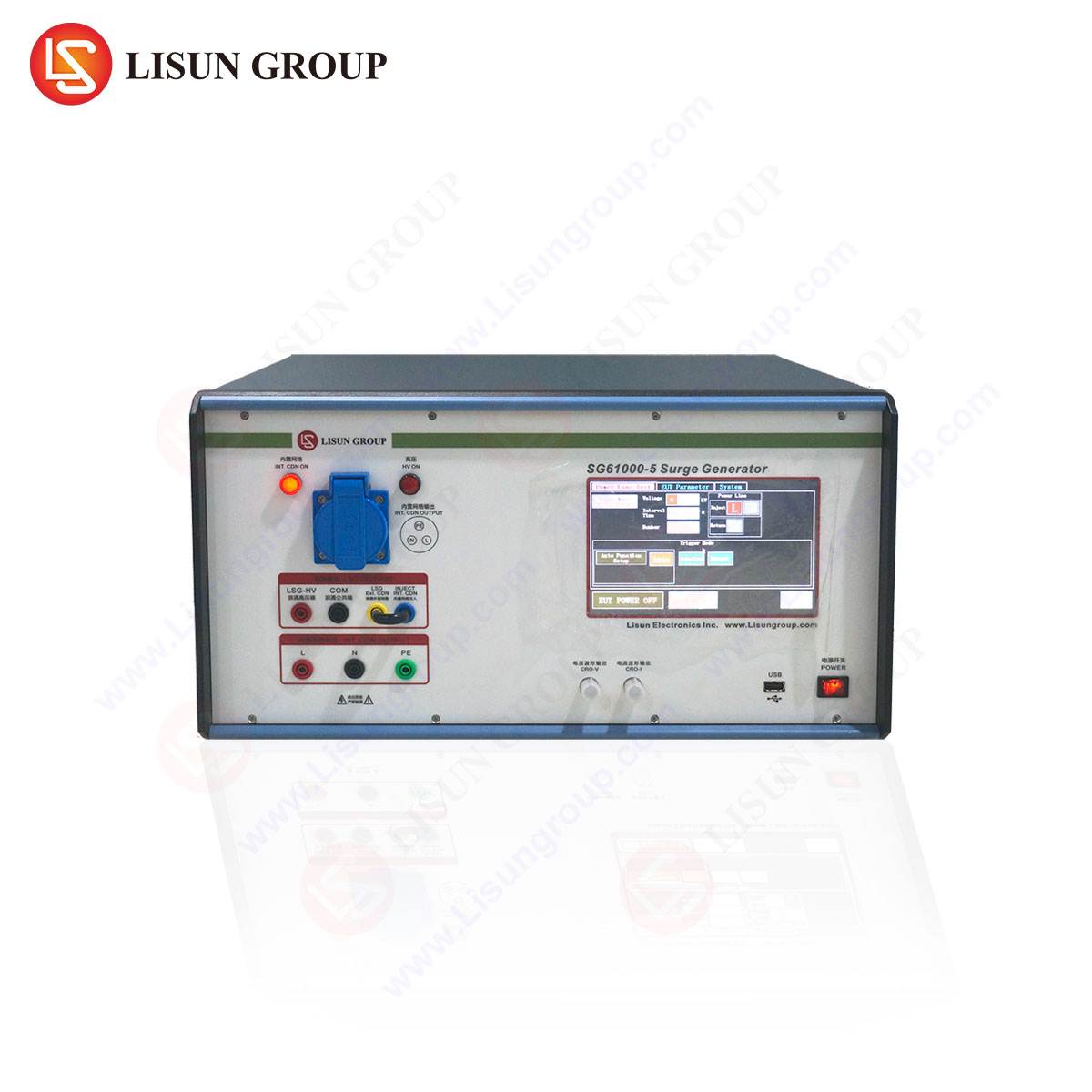
The LISUN ESD61000-2 ESD Simulator: A Benchmark for Validation
While simulation provides predictive insight, physical testing remains the ultimate validation step. The LISUN ESD61000-2 ESD Simulator is engineered to meet and exceed the requirements of the IEC 61000-4-2 standard, providing a reliable and repeatable means of applying ESD stress to equipment.
The ESD61000-2 generates test voltages from 0.1 kV to 30 kV, covering the full range of compliance testing for contact and air discharge methods. Its key performance differentiator lies in its ability to produce the specified IEC 61000-4-2 current waveform with high fidelity. The waveform parameters, including the rise time (0.7-1 ns) and the current levels at 30 ns and 60 ns, are critical for correlating simulation results with physical performance. The instrument features both direct contact discharge and indirect discharge (via a horizontal coupling plane) capabilities, allowing for comprehensive system-level testing.
Table 1: Key Specifications of the LISUN ESD61000-2 Simulator
| Parameter | Specification | Standard |
| :— | :— | :— |
| Test Voltage Range | 0.1 – 30 kV (positive or negative) | IEC 61000-4-2 |
| Discharge Modes | Contact, Air, Indirect | IEC 61000-4-2 |
| Current Waveform | IEC 61000-4-2 | – |
| Rise Time | 0.7 – 1.0 ns | IEC 61000-4-2 |
| Peak Current (at 8 kV) | 15 A ±10% | IEC 61000-4-2 |
| Operational Modes | Single, Repetitive (1-20 Hz) | – |
The testing principle involves charging an energy storage capacitor within the simulator to the desired test voltage and then discharging it through a specified network into the Equipment Under Test (EUT). For Medical Devices and Intelligent Equipment, where functional safety is non-negotiable, the repeatability and accuracy of this discharge are critical for identifying subtle performance degradation or soft errors that may not result in immediate failure but compromise long-term reliability.
Industry-Specific Applications of ESD Simulation and Testing
The application of ESD simulation analysis varies significantly across sectors, dictated by the operational environment, product complexity, and consequence of failure.
In the Automobile Industry, electronic control units (ECUs) for engine management, braking, and infotainment are subjected to ESD events during assembly and from human interaction during vehicle service. Simulation is used to model the discharge path from a touchpoint on the dashboard, through the chassis, and its potential coupling into nearby low-voltage differential signaling (LVDS) cables for displays. The LISUN ESD61000-2 is used to validate the robustness of these systems against the high-voltage transients expected in an automotive environment.
For Household Appliances and Lighting Fixtures with smart touch controls or wireless connectivity, ESD can reset microcontrollers or damage sensitive communication chips like Wi-Fi or Zigbee modules. Simulation helps in optimizing the placement of transient voltage suppression (TVS) diodes and ferrite beads on the PCB. Physical testing with the ESD gun ensures that a user touching a capacitive button does not impair the device’s functionality.
In Medical Devices, such as patient monitors or portable diagnostic equipment, an ESD event could cause a temporary malfunction with critical consequences. Simulation analysis is employed to ensure that sensitive analog front-ends for biosignal acquisition are shielded from both direct discharge and radiated EMI. The ESD61000-2’s precise calibration is essential for verifying that these life-critical devices meet stringent regulatory standards.
The Communication Transmission and Information Technology Equipment sectors rely on high-speed data lines that are exceptionally susceptible to the high-frequency content of an ESD pulse. Simulation models the coupling of energy onto Gigabit Ethernet or USB traces, guiding the design of PCB stack-up, ground plane strategies, and connector shielding. Testing with the simulator confirms the integrity of the data link during and after an ESD strike.
Integrating Simulation and Empirical Testing for Optimal Product Robustness
The most effective ESD mitigation strategy involves a closed-loop process between simulation and physical testing. Simulation is used during the early design phase to explore multiple protection strategies cost-effectively. For instance, a designer for Power Tools can simulate the effect of adding a spark gap or a metal-oxide varistor (MOV) to a motor controller circuit before committing to a PCB layout.
Once a prototype is available, it is subjected to rigorous testing with the LISUN ESD61000-2. The results from this physical testing are then used to correlate and refine the simulation models. Discrepancies between simulated and measured performance often reveal unmodeled parasitic elements or imperfections in the physical layout. This iterative process enhances the predictive accuracy of the simulation models for future product generations, reducing development time and cost.
For Electronic Components and Instrumentation manufacturers, this integration is vital. A chip designer uses simulation to design robust on-chip ESD protection cells. The component is then characterized using specialized ESD testers. The validated component model is subsequently provided to system integrators (e.g., in the Aerospace or Rail Transit industries), who can then use it in their system-level simulations with high confidence, knowing the component’s behavior under ESD stress is accurately represented.
Frequently Asked Questions (FAQ)
Q1: What is the primary advantage of using ESD simulation analysis over proceeding directly to physical testing with a simulator like the LISUN ESD61000-2?
A1: ESD simulation analysis provides a proactive design tool that identifies vulnerabilities during the design phase, before any hardware is built. This allows for rapid, low-cost design iterations and optimization of protection circuits. Physical testing is essential for final validation, but relying on it alone is a reactive process that can lead to expensive and time-consuming PCB re-spins and design changes late in the development cycle.
Q2: For a product with a non-metallic enclosure, such as many Household Appliances, is contact discharge testing still applicable?
A2: Yes, contact discharge is highly applicable. Even on non-conductive surfaces, internal metallic parts, such as PCB ground planes or shielding cans, can become coupled to the ESD event. The IEC 61000-4-2 standard mandates attempting contact discharge on any surface where an air discharge might be unpredictable. The ESD61000-2’s contact discharge mode provides a consistent and repeatable method to stress these points.
Q3: How does the LISUN ESD61000-2 ensure waveform accuracy, and why is this critical?
A3: The ESD61000-2 incorporates a calibrated discharge network and high-voltage components designed to replicate the impedance and energy storage defined by the IEC 61000-4-2 standard. Waveform accuracy is verified using a target and oscilloscope with sufficient bandwidth. An inaccurate waveform, particularly one with an incorrect rise time, will not generate the high-frequency electromagnetic fields representative of a real ESD event, leading to non-representative testing and potentially allowing vulnerable products to pass.
Q4: In the context of ESD simulation, what is the significance of the current discharge path?
A4: The discharge path is the physical route the ESD current takes from the point of injection to the ground reference. In simulation, accurately modeling this path—including the impedance of chassis connections, cables, and PCB grounds—is crucial. The voltage drops along this path, governed by V = L(di/dt), can cause significant ground bounce and are a major source of internal circuit upset. Identifying the path allows designers to widen it, add parallel paths, or place protection devices to steer current away from sensitive areas.