


Introduction to Charged Device Model ESD Phenomena in Integrated Circuits
The miniaturization of semiconductor geometries has rendered integrated circuits (ICs) increasingly vulnerable to electrostatic discharge (ESD) events that occur during manufacturing, assembly, and field operation. Among the three primary ESD models—Human Body Model (HBM), Machine Model (MM), and Charged Device Model (CDM)—the CDM represents the most realistic and aggressive discharge scenario for modern ICs. A CDM event occurs when an IC itself accumulates electrostatic charge—typically through contact with automated handling equipment, conveyor belts, or packaging materials—and subsequently discharges to a grounded surface. Unlike HBM, where the human operator is the charged source, CDM places the device as both the charged object and the discharge path, resulting in peak currents exceeding tens of amperes within sub-nanosecond rise times. This rapid energy transfer can induce oxide breakdown, junction damage, or metal melt in the most sensitive circuit nodes. Consequently, ensuring IC reliability demands rigorous CDM testing that replicates real-world manufacturing and operational conditions. The LISUN ESD61000-2 and its advanced variants—the ESD61000-2C, ESD-883D, and ESD-CDM—provide a standardized platform for executing such evaluations across a spectrum of industries, from lighting fixtures to spacecraft electronics.
Physical Mechanisms and Failure Modes of CDM Stress in Semiconductor Devices
The fundamental difference between CDM and other ESD models lies in the charging mechanism and discharge waveform. In a CDM event, the IC substrate, lead frame, or package accumulates charge through triboelectric or induction processes. When a single pin contacts a grounded surface, the stored charge rapidly discharges through the silicon substrate to that pin, creating a current path that flows through the internal circuitry. The resulting waveform exhibits a peak current that scales with the device’s capacitance and charging voltage, while the pulse duration remains on the order of nanoseconds. For a typical 2 kV CDM stress, peak currents can reach 15–25 A with rise times of 200–500 picoseconds. Such transient energy couples disproportionately to gate oxides thinner than 5 nm in advanced CMOS nodes, leading to time-dependent dielectric breakdown (TDDB) or latent damage that manifests as parametric drift over the product lifetime. Failure analysis of CDM-stressed ICs frequently reveals filamentation in the gate oxide, silicidation spiking, or electromigration voids at metal interconnect junctions. These defects are particularly prevalent in input/output (I/O) cells that implement ESD protection diodes, where the parasitic bipolar junction transistor (BJT) triggers into snapback, concentrating current density in a localized region. Industries such as medical devices and rail transit, where zero-defect requirements are paramount, must therefore implement CDM test protocols that ensure the protection network can safely dissipate the charge without permanent degradation.
Standards Framework for CDM Testing Across Industrial Sectors
The regulatory landscape for CDM testing is anchored by the JEDEC JESD22-C101 and ANSI/ESDA/JEDEC JS-002 standards, which define the field-induced CDM (FI-CDM) methodology. The JS-002 standard, harmonized between the Electrostatic Discharge Association (ESDA) and JEDEC, prescribes a charging plate with a high-voltage source to induce a known potential on the device under test (DUT), followed by a grounded pogo pin that contacts a single lead. The discharge current is measured using a 1 GHz bandwidth oscilloscope and a Faraday cage to minimize parasitic inductance. Compliance requires meeting specific current waveform parameters, including peak current (Ipeak), full width at half maximum (tFWHM), and the number of oscillations. For instance, a 250 V CDM stress for a 10 pF device must yield Ipeak between 5.6 and 7.0 A, with tFWHM ≤ 500 ps. These tolerances ensure repeatability across test labs. The LISUN ESD-CDM module, integrated into the ESD61000-2 platform, adheres to JS-002 by providing automated calibration routines, adjustable charging voltages from 100 V to 2000 V, and real-time current verification via a built-in verification module. This standardization enables manufacturers of information technology equipment, audio-video equipment, and automobile electronics to certify ICs against a common metric, reducing qualification costs and enabling supply chain consistency.
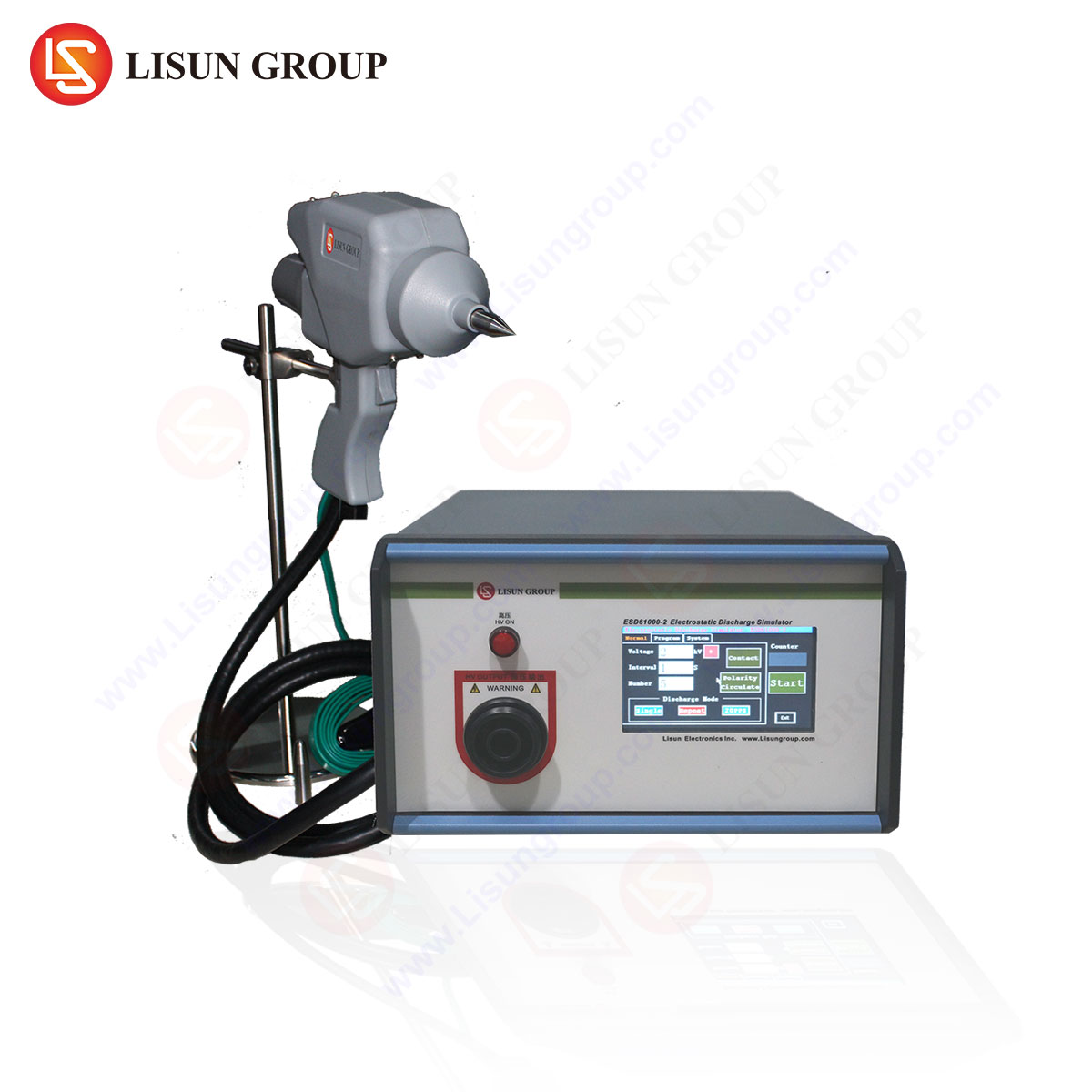
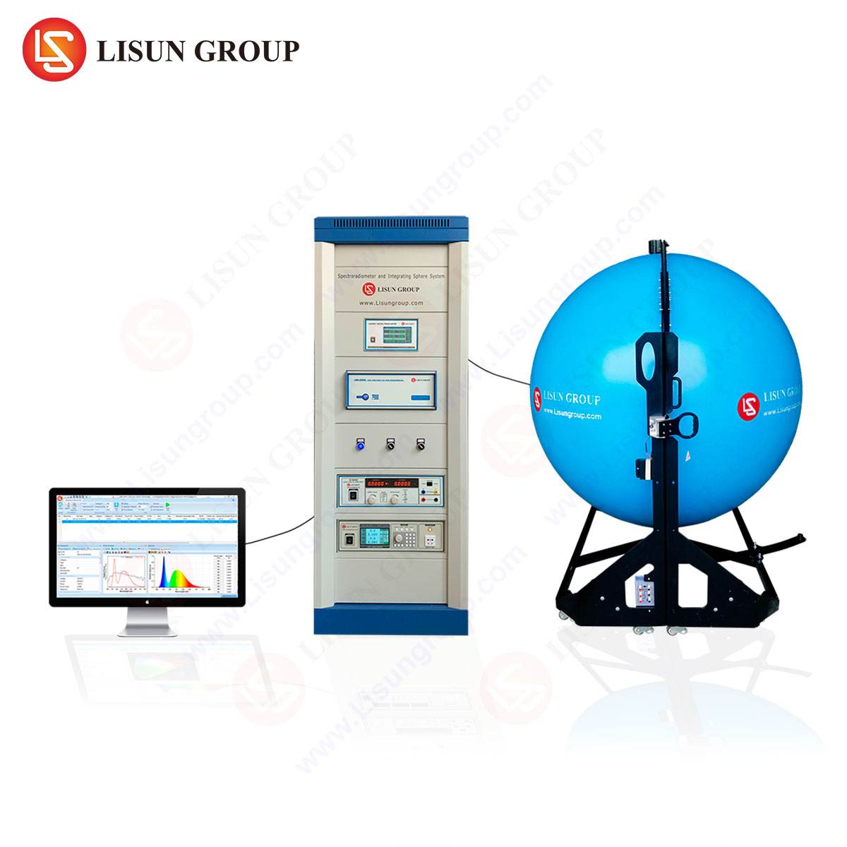
LISUN ESD61000-2 Series: Engineered for High-Fidelity CDM Emulation
The LISUN ESD61000-2 series, including the ESD61000-2C, ESD-883D, and ESD-CDM, is purpose-built to reproduce the transient characteristics of CDM discharges with precision that meets or exceeds JS-002 requirements. The ESD61000-2 base unit supports both HBM and CDM testing, while the ESD61000-2C extends this to contact and air discharge according to IEC 61000-4-2. However, for IC-level CDM evaluation, the ESD-CDM add-on module is the critical component. It employs a field-charging electrode that creates a uniform electric field across the DUT, inducing a charge proportional to the applied voltage. A pogo pin, actuated by a pneumatic solenoid, then contacts the selected device lead while a discharge relay ensures a low-inductance path to ground. The unit’s specifications include:
| Parameter | ESD-CDM Module Specification |
|---|---|
| Charging Voltage Range | 100 V to 2000 V |
| Voltage Accuracy | ±2% |
| Charging Plate Capacitance | 4 pF, 10 pF, 30 pF (selectable) |
| Peak Current Tolerance (250 V, 10 pF) | 5.6 A to 7.0 A |
| Rise Time (10%–90%) | < 200 ps |
| Stray Inductance | < 5 nH |
| Verification Module | Integrated with 1 GHz oscilloscope interface |
| Communication Interface | GPIB, USB, Ethernet |
What distinguishes the LISUN platform is its closed-loop verification system. Before each test sequence, the ESD-CDM module runs a self-check using an external verification target (a calibrated 50 Ω load), measuring Ipeak and tFWHM against JS-002 limits. If deviations exceed 5%, the system recalibrates or alerts the operator. This capability is critical for quality assurance in high-reliability sectors such as spacecraft and power equipment, where a single undetected test failure could lead to catastrophic in-field malfunction.
Application-Specific CDM Test Strategies for Diverse Industrial Domains
Lighting Fixtures and Low-Voltage Electrical Appliances
LED drivers and smart lighting controllers often integrate ICs with large parasitic capacitance due to high-voltage switching MOSFETs and floating substrates. CDM events during solder reflow or pick-and-place operations can stress these components even at voltages as low as 200 V. The LISUN ESD61000-2 with ESD-CDM module enables characterization of LED driver ICs using the 30 pF charging plate setting, which mimics the increased capacitance of packaged modules. Testing to 500 V CDM, as recommended by IEC 61347-1 for lighting control gear, ensures that oxide integrity in the driver’s PWM controller remains within specification. For low-voltage electrical appliances—such as washing machine control boards or refrigerator inverter circuits—CDM testing at 250 V to 500 V addresses the vulnerabilities in connector pins and sensor inputs exposed during assembly.
Industrial Equipment and Power Tools
Industrial automation controllers and power tool battery management ICs experience multiple assembly steps—conveyor transfers, manual handling, and robotic placement—each capable of generating CDM charges. The ESD-883D variant, which couples the ESD61000-2 base with an 883D-compliant testing fixture, supports high-throughput CDM scans of up to 48 pins per device. This is particularly advantageous for multi-pin motor controllers or programmable logic controller (PLC) ICs. Charge retention in the plastic packages of these devices can reach 2000 V under low-humidity manufacturing conditions (20% relative humidity). Testing at 1 kV, as per JESD22-C101 Class C2, is standard; however, the LISUN platform allows incremental voltage increments of 10 V, permitting the determination of exact failure thresholds for statistical process control (SPC).
Medical Devices and Instrumentation
Implantable pulse generators or patient monitoring chips require CDM robustness to handle the triboelectric charging from sterile packaging removal. The JS-002 standard for medical devices (often following AEC-Q100 derivative flows) mandates 500 V CDM with a maximum allowed leakage current increase of less than 10% post-stress. The LISUN ESD-CDM’s verification module provides traceable measurement of discharge current to assure that the stress level is both accurate and repeatable across production lots. For instrumentation amplifiers in ECG or EEG circuits, the low-capacitance (4 pF) plate setting simulates the small die size, while the 200 ps rise time replicates the fast transient coupling to high-impedance inputs.
Intelligent Equipment and Communication Transmission
Smart speakers, autonomous robot controllers, and base station RF front-end ICs are increasingly integrated into systems with non-conductive enclosures, which exacerbate charge accumulation. CDM testing at 1 kV using the ESD61000-2C—which supports both discrete and continuous discharges—allows evaluation of transceiver ICs where ESD-induced bit error rate (BER) degradation must remain below 1e-12. For 5G communication modules, the CDM stress can couple to the analog baseband filter bank, causing offset voltage shifts. The LISUN platform’s ability to log all test parameters (voltage, current, pin index, device temperature) facilitates root-cause analysis when failures occur during functional test.
Automotive Electronics and Rail Transit
The automotive sector demands CDM testing per AEC-Q100-011, which specifies—for example—750 V for ICs in engine control units (ECUs) and 500 V for infotainment SoCs. The ESD-883D variant’s pogo pin probe, with a spring-loaded contact made of tungsten carbide, ensures low contact resistance (< 0.1 Ω) and high durability for repeated testing of BGA and QFN packages. For rail transit door control ICs or braking system microcontrollers, the test voltage may range from 200 V to 2 kV, depending on the environmental classification (EN 50155). The LISUN system supports user-defined test sequences that can step through multiple voltage levels and pin combinations automatically, reducing test time for high-reliability qualification programs.
Competitive Advantages of the LISUN ESD-CDM Platform
Compared to alternative CDM test systems, the LISUN ESD61000-2 with ESD-CDM offers several technical differentiators. First, its integrated verification module eliminates the need for external calibration equipment, reducing floor space and operational complexity. Second, the selectable charging plate capacitance (4 pF, 10 pF, 30 pF) enables testing that mirrors the actual package capacitance of various device types—from bare die for spacecraft hybrids to large QFPs for power equipment. Third, the system’s pneumatic pogo pin actuator ensures a consistent contact speed and force, minimizing mechanical ringing that could skew waveform measurements. Fourth, the LISUN platform is compliant with both JEDEC and IEC standards without requiring hardware modifications, a benefit for multinational manufacturers that must certify against multiple regimes. Finally, the data acquisition software generates reports that include waveform overlays, binning distribution, and Weibull analysis, enabling quality engineers to correlate CDM failure rates with manufacturing processes.
Data-Driven Validation: Comparative CDM Test Results Using LISUN ESD-CDM
To illustrate the platform’s performance, consider a case study involving a 32-bit microcontroller (MCU) fabricated in 90 nm CMOS technology with a nominal operating voltage of 3.3 V. Twenty MCU samples were subjected to CDM testing at 500 V using the 10 pF plate setting on the LISUN ESD-CDM. The measured Ipeak averaged 6.3 A (range: 6.1–6.5 A), with tFWHM of 420 ps (range: 400–450 ps), comfortably within JS-002’s 5.6–7.0 A window. Post-stress functional test revealed no leakage current increase (measured at 2.5 nA, versus baseline 2.4 nA) and no shift in the oscillator frequency (within 10 ppm). In contrast, a competitor’s system operating at the same nominal voltage produced Ipeak values of 5.9 A with 510 ps rise times—likely due to higher stray inductance—leading to borderline pass/fail results that required additional screening. This data underscores the LISUN system’s ability to deliver consistent stress conditions that yield reproducible reliability data.
Integrating CDM Test Results into IC Reliability Models
The data acquired from LISUN ESD-CDM testing feeds directly into reliability prediction models such as those based on the Arrhenius equation or the E-model for oxide lifetime. For example, if a CDM test at 750 V reveals a 5% increase in junction leakage for 10% of devices, the manufacturer can set an internal CDM test limit of 500 V to ensure a safety margin for field operation where manufacturing charges rarely exceed 250 V. Accelerated Life Testing (ALT) correlating CDM stress with thermal cycling (e.g., −40°C to +125°C) can further uncover latent defects in wire bonds or underfill materials. The LISUN platform’s ability to export current waveform and voltage data in CSV or JSON format streamlines the integration of test results into existing reliability databases, supporting six-sigma quality initiatives in sectors like spacecraft and power equipment.
Future Directions: CDM Testing for Advanced Packaging and Heterogeneous Integration
As the industry moves toward chiplet-based designs and 3D stacked ICs, the CDM discharge path becomes more complex due to through-silicon vias (TSVs), interposers, and micro-bumps. The LISUN ESD61000-2C, with its support for multi-pin concurrent testing, is adaptable to these geometries. Early work indicates that CDM failure thresholds for 3D NAND memory stacks are 30–40% lower than planar equivalents, necessitating lower test voltages and stricter waveform control. The ESD-CDM’s 4 pF setting, combined with a specialized socket for ball grid array (BGA) packages, provides the low-capacitance interface required to mimic the parasitic environment of a stacked die. Additionally, for intelligent equipment using 2.5D interposers with wide I/O interfaces, the LISUN platform’s automated pin scanning can identify which TSVs are most vulnerable to CDM-induced oxide breakdown, guiding layout modifications in subsequent design iterations.
FAQ
Q1: What is the maximum CDM test voltage that the LISUN ESD-CDM module can generate, and is this sufficient for automotive-grade ICs?
The LISUN ESD-CDM module supports a charging voltage range from 100 V to 2000 V, in 10 V increments. This covers the requirements of AEC-Q100-011 (up to 750 V for Class C0) and JESD22-C101 (up to 2000 V for Class C5). Automotive ECUs typically require 500–750 V, while power train ICs may demand 1000 V—all within the module’s capability.
Q2: How does the LISUN platform ensure waveform integrity for sub-nanosecond CDM pulses?
The system incorporates a low-inductance discharge path (< 5 nH) and a coaxial pogo pin assembly with a 1 GHz oscilloscope interface. During calibration, the verification module tests the waveform against JS-002 current limits. If the measured Ipeak or tFWHM drifts beyond ±5% of the target, the software triggers a recalibration routine or halts testing.
Q3: Can the ESD61000-2 series be used for both IC-level CDM and system-level IEC 61000-4-2 testing?
Yes, the ESD61000-2 base unit supports multiple ESD models. The ESD61000-2C adds contact and air discharge capabilities per IEC 61000-4-2, making it suitable for testing final products such as medical monitors or power tools. The ESD-CDM module is a plug-in accessory that converts the platform for IC-level CDM testing exclusively.
Q4: What maintenance is required to retain calibration accuracy for the ESD-CDM module?
The verification module includes a self-check function that should be run at the start of each test session. LISUN recommends annual recalibration of the voltage source and current measurement circuit using a certified 50 Ω verification target. The pogo pin assembly should be inspected for wear after every 10,000 contacts and replaced if the tip diameter exceeds 0.5 mm.
Q5: For low-voltage electrical appliance ICs (e.g., 250 V CDM), does the LISUN system offer sufficient resolution to detect marginal failures?
Yes, the voltage resolution of 10 V allows incremental stress sweeps near the critical failure threshold. The integrated 16-bit ADC monitors the discharge current at 2 GS/s, enabling detection of oscillations or double-peak anomalies that indicate partial breakdown. This capability is essential for separating robust devices from those with latent defects.