


A Comprehensive Framework for Electrostatic Discharge Protection in Modern Electronic Systems
Introduction
The pervasive integration of sensitive semiconductor devices across industrial and consumer sectors has rendered Electrostatic Discharge (ESD) protection a critical pillar of product reliability and safety. ESD events, characterized by transient, high-current discharges, can induce catastrophic failure or latent damage in integrated circuits, leading to field returns, safety hazards, and reputational damage. A robust ESD protection design is not an ancillary consideration but a fundamental requirement, spanning from the component level to the final system enclosure. This article delineates a systematic methodology for ESD protection design, validated through rigorous compliance testing, with a focus on the instrumental role of advanced test equipment such as the LISUN ESD61000-2C ESD Simulator in qualifying designs against international standards.
Fundamental ESD Failure Mechanisms in Semiconductor Components
Understanding the physics of ESD-induced failure is prerequisite to effective protection. ESD stress manifests primarily through three damage models: thermal, dielectric, and metallization failure. The Human Body Model (HBM) and Charged Device Model (CDM) represent the most prevalent stress paradigms. HBM simulates a discharge from a human operator, typically a current pulse with a rise time of 2-10 nanoseconds and a decay of approximately 150 nanoseconds, which can cause junction spiking and metallization melt due to localized Joule heating. CDM, often more severe for modern, high-speed components, simulates the rapid discharge from a charged device itself, producing sub-nanosecond rise times and peak currents exceeding 10 Amperes. This can puncture thin gate oxides or cause charge trapping, leading to parametric shifts. For industries like Automotive Industry and Medical Devices, where functional safety is paramount, latent CDM damage poses a significant risk, as it may not cause immediate failure but degrade performance over time, potentially with critical consequences.
Hierarchical Protection Strategy: From System Enclosure to IC Pad
Effective ESD mitigation employs a layered, or hierarchical, defense strategy. The primary layer involves preventing charge accumulation and providing a safe discharge path at the system level. This includes the use of conductive or static-dissipative materials in enclosures for Industrial Equipment and Household Appliances, proper earth bonding of metal chassis in Power Equipment and Rail Transit vehicles, and the implementation of spark gaps or transient voltage suppression (TVS) diodes on communication ports (e.g., RS-485, CAN bus) in factory automation systems.
The secondary layer focuses on printed circuit board (PCB) design. Key practices include minimizing loop areas for high-frequency discharge currents, using ground planes to provide low-inductance return paths, and implementing series resistors or ferrite beads on signal lines to limit current. For interfaces in Audio-Video Equipment and Communication Transmission gear, such as HDMI or Ethernet, careful placement of board-level TVS arrays with low capacitance is essential to protect high-speed transceivers without signal integrity degradation.
The tertiary and most critical layer is the on-chip protection network integrated within the Electronic Components themselves. These networks, typically comprising snapback or clamp devices, must trigger rapidly (often in picoseconds) to shunt the ESD current away from the sensitive core circuitry. The design must balance holding voltage, trigger voltage, and current-handling capability, often characterized by Transmission Line Pulse (TLP) testing, to ensure robustness without interfering with normal operation.
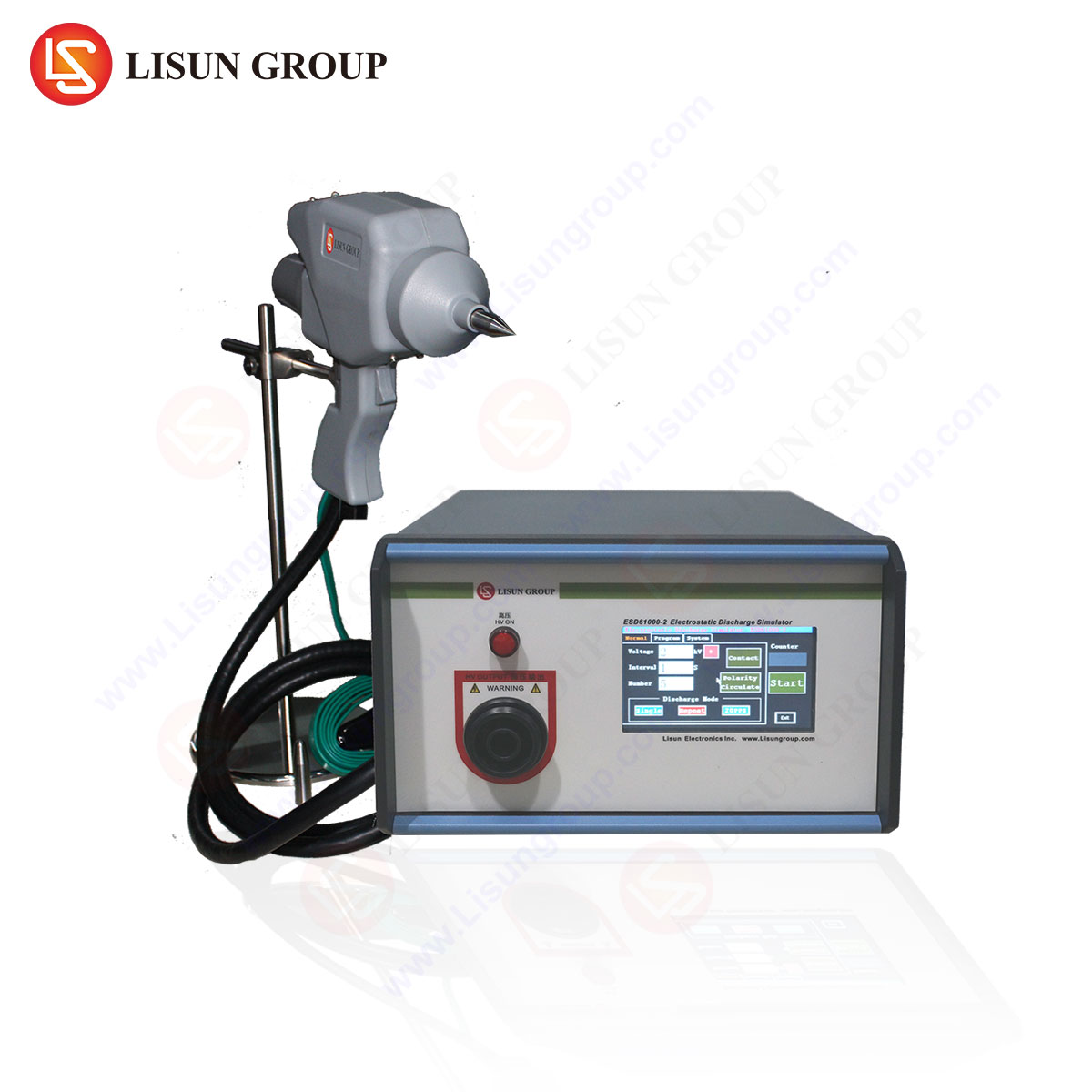
Validation Through Standardized Testing: The Role of the LISUN ESD61000-2C Simulator
Design validation necessitates testing against standardized ESD waveforms. The LISUN ESD61000-2C ESD Simulator is a state-of-the-art instrument engineered for compliance testing per IEC 61000-4-2, the principal international standard for system-level ESD immunity. Its specifications define its capability to accurately replicate real-world discharge events.
- Test Voltage Range: 0.1 kV to 30 kV (air discharge) and 0.1 kV to 30 kV (contact discharge), covering all severity levels specified in standards for products from Low-voltage Electrical Appliances to Information Technology Equipment.
- Discharge Current Waveform: The generator is calibrated to produce the stringent current waveform defined by IEC 61000-4-2: a rise time of 0.7-1.0 ns and specific current values at 30 ns (e.g., 16.8 A for 4 kV contact discharge) and 60 ns. Accurate waveform generation is non-negotiable for reproducible, credible test results.
- Testing Principles: The simulator operates in two primary modes. Contact discharge testing, used for conductive surfaces, employs a sharp discharge tip that contacts the Equipment Under Test (EUT) before the discharge is initiated. Air discharge testing, for insulated surfaces, uses a rounded tip; the voltage is increased until an arc bridges the air gap to the EUT, simulating a spark from a human finger. The ESD61000-2C features advanced functions like automatic voltage grading, real-time waveform monitoring, and comprehensive test logging, which are indispensable for efficient qualification testing in laboratories serving the Lighting Fixtures, Instrumentation, and Power Tools sectors.
Integrating ESD61000-2C Testing into the Product Development Lifecycle
The use of the ESD61000-2C should be integrated early and throughout the development process. During the design phase, pre-compliance testing on prototype boards helps identify vulnerabilities in enclosure design, grounding schemes, and PCB layout. For a Medical Device such as a patient monitor, testing would focus on all user-accessible points, including touchscreens, buttons, and data ports, ensuring no disruption to critical monitoring functions.
In the validation phase, full compliance testing is conducted according to the relevant product family standard (e.g., IEC 60601-1-2 for medical, ISO 10605 for automotive, IEC 61000-6-2 for industrial environments). The tester’s programmability allows for the execution of complex test sequences, applying specified numbers of discharges at both positive and negative polarities to each test point. For Intelligent Equipment and Communication Transmission base stations, which must operate in harsh environments, testing often includes discharges under varied climatic conditions (temperature, humidity) to assess performance margins.
Competitive Advantages of Precision ESD Testing Equipment
The competitive landscape for ESD simulators demands instruments that offer not just compliance, but also reliability, usability, and data integrity. The LISUN ESD61000-2C exemplifies this through several key advantages. Its high-stability high-voltage source ensures minimal voltage droop during repetitive discharges, guaranteeing consistent stress application. Integrated real-time current waveform verification via a built-in or external target provides immediate feedback on the quality of the discharge, a critical feature for accredited test labs. Furthermore, its software interface facilitates the creation, execution, and documentation of test plans, streamlining the process for industries with stringent traceability requirements, such as the Automobile Industry and Spacecraft component suppliers, where test records are part of the mandatory product dossier.
Material Science and Component Selection for ESD Hardening
The selection of materials and discrete protection components is a science in itself. For enclosures, the surface resistivity of plastics is critical: conductive materials (< 1 x 10⁵ Ω/sq) quickly equalize charge, while dissipative materials (1 x 10⁵ to 1 x 10⁹ Ω/sq) control the discharge rate. In Household Appliances with electronic control panels, dissipative coatings can prevent charge buildup from user interaction without creating a shock hazard.
At the circuit level, selection of TVS diodes requires analysis of key parameters: working voltage, breakdown voltage, clamping voltage, peak pulse current (Ipp), and junction capacitance. For high-speed data lines in Audio-Video Equipment (e.g., USB 3.0, DisplayPort), diodes with capacitance below 0.5 pF are mandatory. For high-energy transients in Power Equipment or Industrial Equipment motor drives, silicon avalanche suppressors or metal-oxide varistors (MOVs) with high Ipp ratings are employed. Polymer-based positive temperature coefficient (PTC) devices can be used in series for resettable current limiting.
Case Study: ESD Protection in an Automotive Infotainment System
Consider the development of an automotive infotainment unit, a convergence of Automobile Industry robustness and Information Technology Equipment complexity. The system faces ESD threats from user touchscreens, USB ports, SD card slots, and external antenna connections. The protection strategy would be multi-faceted:
- Enclosure & UI: The touchscreen would incorporate a transparent, static-dissipative coating. All knobs and buttons would have limited internal travel and, where possible, conductive springs bonded to chassis ground.
- PCB & Interfaces: The main PCB would feature a continuous ground plane. Each external port would be protected by a dedicated array of low-capacitance TVS diodes (e.g., for USB D+/D- lines) and higher-capacitance TVS or varistors for power lines. The FM/AM antenna input would use a gas discharge tube (GDT) in series with a TVS diode to handle very high voltages induced from nearby lightning strikes.
- On-Chip Protection: The system-on-chip (SoC) for multimedia processing and the CAN transceiver for vehicle communication would be sourced with a high level of inherent HBM and CDM protection (e.g., ≥ 2 kV HBM, ≥ 500 V CDM).
This design would be rigorously validated using an ESD61000-2C simulator, performing both contact discharge to metallic trim and air discharge to the screen and plastic surfaces, per ISO 10605 test procedures, which specify different RC networks than IEC 61000-4-2 to better represent the automotive environment.
Future Trends and Challenges in ESD Protection Design
The evolution of technology presents continuous challenges for ESD protection. The proliferation of wide-bandgap semiconductors (SiC, GaN) in Power Equipment and electric vehicle chargers operates at higher temperatures and switching speeds, requiring protection devices with matching thermal stability and faster response. The miniaturization of Electronic Components following Moore’s Law results in thinner gate oxides more susceptible to CDM, pushing on-chip protection design to its limits. Furthermore, the rise of the Internet of Things (IoT) in Intelligent Equipment and Household Appliances means more devices with exposed antennas and low-cost plastic enclosures are deployed in uncontrolled environments, increasing ESD exposure risk. These trends underscore the enduring necessity for sophisticated design strategies and the precise, reliable validation provided by advanced test equipment like the LISUN ESD61000-2C.
Frequently Asked Questions (FAQ)
Q1: What is the critical difference between contact discharge and air discharge testing with the ESD61000-2C, and how do I choose the correct method?
A1: Contact discharge testing is applied to conductive surfaces accessible to the user. The discharge tip is held in contact with the EUT, and the discharge is initiated directly, providing highly repeatable results. Air discharge simulates a spark over an air gap to insulated surfaces. The choice is dictated by the product standard and the materials of the EUT. Most standards, like IEC 61000-4-2, mandate contact discharge where applicable, resorting to air discharge for non-conductive surfaces.
Q2: For a medical device requiring compliance with IEC 60601-1-2, what test levels from the ESD61000-2C are typically required?
A2: IEC 60601-1-2 references IEC 61000-4-2. For medical electrical equipment, the standard typically specifies a minimum test level of ±3 kV for contact discharge and ±8 kV for air discharge for equipment not classified as “life-supporting.” For life-supporting equipment, stricter criteria, often requiring higher performance levels (e.g., with no degradation during test), are applied at these same voltages. The specific applicable level is defined in the device’s risk analysis and essential performance criteria.
Q3: How does the ESD61000-2C assist in troubleshooting a failed ESD test?
A3: The instrument’s capabilities are crucial for fault diagnosis. Its real-time waveform display can verify that the correct stress was applied. By using its programmable test sequences, an engineer can isolate the failing test point and polarity. Coupled with diagnostic monitoring of the EUT (e.g., using software to log errors), one can determine if the failure was a hard reset (requiring improved power rail protection or microcontroller watchdog circuit) or a soft functional error (indicating inadequate signal line protection or software susceptibility).
Q4: Can the ESD61000-2C simulator be used for testing components directly, in addition to finished systems?
A4: While its primary design is for system-level testing per IEC 61000-4-2, it can be used for qualitative component-level stress testing, such as evaluating the robustness of a connector or a discrete TVS diode on a evaluation board. However, for formal qualification of semiconductor components to HBM or CDM standards (e.g., JS-001, JESD22-C101), dedicated component-level ESD testers with different output networks and waveform verification methods are required.