


Understanding the Charged Device Model: A Critical Electrostatic Discharge Failure Mechanism in Modern Electronics
Introduction to Device-Level Electrostatic Discharge Phenomena
Electrostatic Discharge (ESD) represents a persistent and formidable threat to the integrity and reliability of electronic components and systems across all industrial sectors. While several standardized models exist to simulate ESD events, the Charged Device Model (CDM) has emerged as the predominant cause of latent and catastrophic failures in contemporary high-density, high-speed integrated circuits and assembled printed circuit boards (PCBs). Unlike the Human Body Model (HBM), which simulates a discharge from a human to a device, CDM characterizes the event wherein a device itself becomes triboelectrically charged and subsequently discharges rapidly to a grounded conductor. This discharge event, characterized by an extremely fast rise time and high peak current, directly impacts internal device structures, often with devastating consequences. A comprehensive understanding of CDM ESD, its underlying physics, testing methodologies, and mitigation strategies is therefore indispensable for design engineers, quality assurance professionals, and reliability specialists engaged in the development of robust electronic products.
The Physics of Charge Accumulation and Discharge in CDM Events
The genesis of a CDM event is rooted in triboelectric charging. During manufacturing, handling, or transportation, electronic devices—whether individual components like integrated circuits (ICs) or assembled boards—can come into contact with and then separate from various materials such as conveyor belts, trays, foam, or packaging. This contact and separation process results in a net transfer of charge, leaving the device at an electrostatic potential relative to its surroundings. The magnitude of this potential can easily reach several kilovolts.
When this charged device approaches a grounded conductor or a conductor at a different potential, the electric field between them intensifies. Upon reaching a critical threshold, the air (or other insulating medium) breaks down, and the charge on the device redistributes to the conductor via a spark or a direct conductive path. The critical distinction from HBM is the discharge pathway: in CDM, the current flows from the device into the ground, traversing the device’s internal pins and circuitry. The equivalent circuit is primarily the device’s own capacitance to its surroundings (C_CDM) discharging through its internal resistance and inductance, and the resistance of the spark or contact.
The resulting current waveform is exceptionally fast, with rise times typically in the range of 200 to 500 picoseconds and total pulse durations of 1 to 2 nanoseconds. Peak currents can exceed 10 Amperes for a 500V CDM event on a typical IC package. This ultrafast, high-current pulse injects energy directly into sensitive oxide layers, junction structures, and interconnects within the semiconductor die, leading to failure modes distinct from those caused by slower ESD models.
Distinctive Failure Mechanisms Induced by CDM Stress
The unique transient nature of the CDM pulse precipitates specific failure mechanisms that often evade detection during HBM testing. The high current density and speed cause localized heating and dielectric breakdown at points of high electric field concentration within the device.
Primary CDM failure sites include gate oxide breakdown in metal-oxide-semiconductor (MOS) transistors, where the thin insulating layer is punctured by the high voltage transient. Junction spiking and melting occur at source/drain regions due to localized current crowding and subsequent thermal runaway. Additionally, damage to shallow trench isolation (STI) and metallization layers, including via and contact burnout, is common. These failures are frequently latent, manifesting as parametric shifts (e.g., increased leakage current, altered threshold voltage) or functional intermittency only after the device has been in operation for some time, posing a severe reliability risk. For industries such as Medical Devices, Automotive Industry, and Spacecraft, where failure is not an option, latent CDM failures represent a critical concern that must be addressed through rigorous testing.
Standardized Testing Methodologies for CDM Qualification
To ensure component and assembly robustness, international standards bodies have defined precise test methods for CDM. The most widely recognized standard is the ANSI/ESDA/JEDEC JS-002, “Charged Device Model (CDM) – Component Level.” This standard specifies the test apparatus, calibration procedure, and test protocol. The test involves placing the Device Under Test (DUT) on a field plate with its leads facing upward, charging it to a specified voltage via a high-voltage supply, and then initiating the discharge through a grounded pogo pin that contacts a selected pin of the DUT. The discharge current waveform is monitored using a high-bandwidth measurement system to verify compliance with the standard’s target waveform parameters.
Testing is performed on all relevant pin combinations to simulate real-world discharge scenarios. Passing criteria are defined by the component manufacturer or customer requirements, typically requiring zero catastrophic failures and parametric shifts within specified limits after exposure to CDM stress levels ranging from 250V to 2000V, depending on the device’s sensitivity and application environment. Compliance with JS-002 or its equivalents is a mandatory requirement for component suppliers serving the Information Technology Equipment, Communication Transmission, and Electronic Components industries.
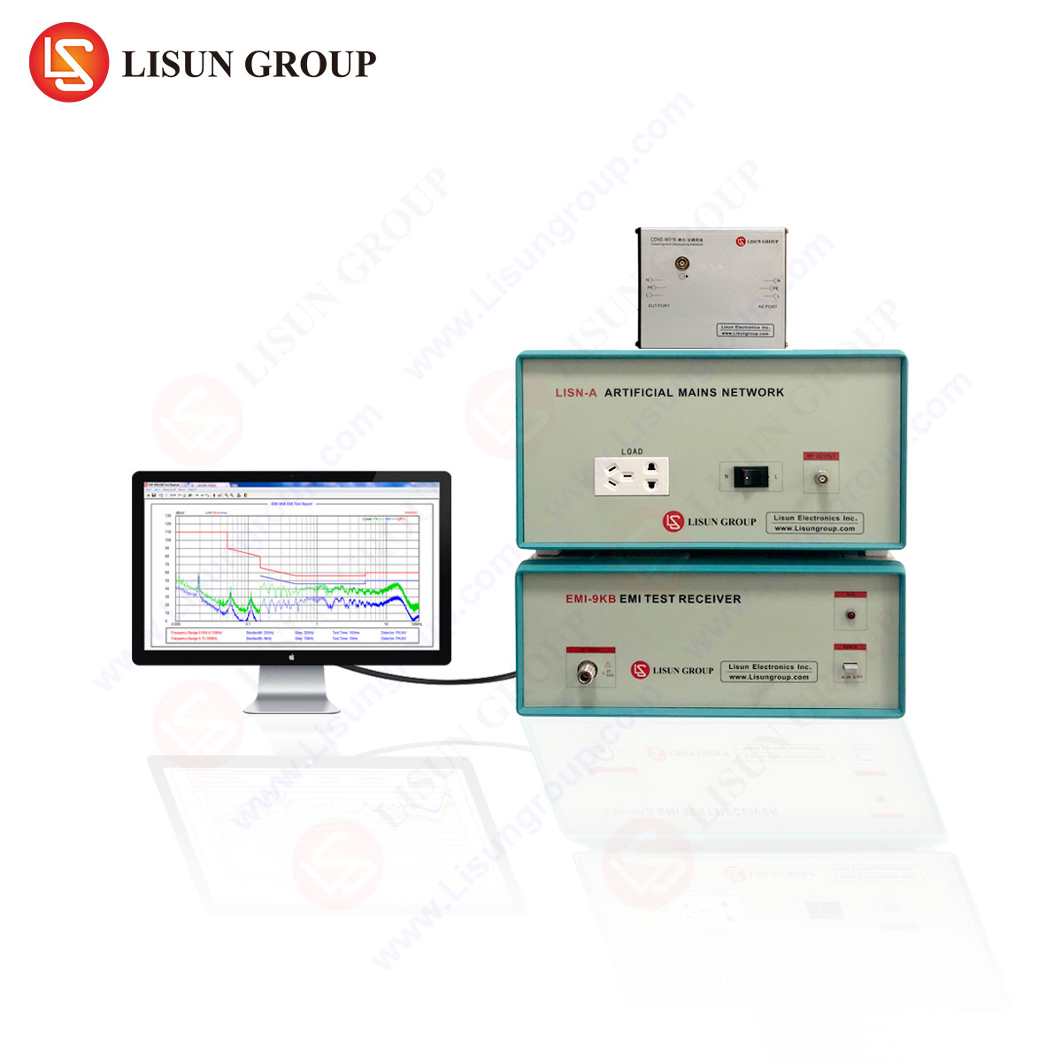
The LISUN ESD-CDM Simulator: Precision in Component-Level ESD Validation
Accurate and repeatable CDM testing necessitates instrumentation capable of generating the nanosecond-scale waveforms defined by industry standards. The LISUN ESD-CDM Electrostatic Discharge Simulator is engineered specifically to meet the rigorous demands of JS-002 and related standards, providing a reliable solution for component manufacturers and qualification laboratories.
The testing principle of the LISUN ESD-CDM simulator centers on its ability to precisely control the charge voltage applied to the DUT and to deliver a consistent, standardized discharge through a low-inductance relay and pogo pin assembly. The system features a high-precision high-voltage DC power supply for charging, a calibrated discharge head, and integrated current waveform verification tools. Its design minimizes parasitic inductance and capacitance in the discharge path, ensuring the generated waveform faithfully replicates the fast-rising, high-current pulse of a real CDM event.
Specifications and Competitive Advantages of the LISUN ESD-CDM System
Key specifications of the LISUN ESD-CDM simulator include a wide test voltage range (typically from 125V to 2000V or higher), polarity switching capability, and a discharge rise time compliant with JS-002 requirements (<500 ps). The system incorporates automated test sequencing, allowing for efficient testing of multiple pins on a device, and includes sophisticated software for waveform monitoring, data logging, and report generation.
The competitive advantages of this system are multifold. First, its high measurement accuracy and repeatability ensure reliable qualification data, reducing false passes or failures. Second, the robust and user-friendly design enhances laboratory throughput and operational safety. Third, its full compliance with international standards guarantees that test results are recognized and accepted across global supply chains. For manufacturers of Instrumentation, Power Equipment, and Rail Transit control systems, utilizing a validated tool like the LISUN ESD-CDM is essential for certifying the ESD robustness of critical components.
Industry-Specific Applications and Use Cases for CDM Testing
CDM susceptibility is a universal concern, but its implications vary by sector.
In the Automotive Industry, electronic control units (ECUs), sensors, and infotainment systems are subjected to automated handling during assembly. CDM testing of components like microcontrollers and power MOSFETs is critical to prevent field failures that could affect safety systems.
For Medical Devices, implantable electronics and portable diagnostic equipment must maintain absolute functional integrity. Latent CDM damage in an analog front-end chip or a wireless communication module could lead to erroneous readings or loss of function, with direct implications for patient safety.
Household Appliances and Power Tools increasingly incorporate sophisticated motor drives and touch interfaces. CDM robustness ensures that these products can withstand the charging that occurs during automated PCB assembly and final product assembly without degraded performance.
In Lighting Fixtures, particularly LED drivers and smart lighting controllers, CDM failures can cause immediate short circuits or gradual efficiency loss. Similarly, Industrial Equipment and Power Equipment rely on robust gate drivers and IGBTs where CDM-induced oxide damage can lead to catastrophic failure under high-voltage, high-current operating conditions.
Communication Transmission and Audio-Video Equipment utilize high-frequency, low-voltage components extremely sensitive to fast transients. CDM testing validates the resilience of SerDes interfaces, RF amplifiers, and high-speed memory devices.
Finally, in the most demanding environments of Spacecraft and Aerospace, where repair is impossible, CDM qualification of every electronic component is a non-negotiable part of the reliability assurance program, often requiring testing to levels beyond commercial standards.
Mitigation Strategies Across the Product Lifecycle
Combating CDM failures requires a holistic approach spanning design, manufacturing, and handling.
At the component design level, incorporation of robust CDM-specific on-chip protection circuits at every pin is paramount. These circuits must be optimized for the fast CDM pulse, often requiring distributed protection networks and low-impedance clamp elements.
During PCB Assembly and device manufacturing, strict electrostatic protected area (EPA) controls are necessary. This includes the use of conductive or dissipative worksurfaces, grounded personnel via wrist straps, ionizers to neutralize charge on insulating materials, and the use of CDM-safe packaging and trays that prevent charge accumulation on devices.
For end-product assembly in industries like Intelligent Equipment or Low-voltage Electrical Appliances, ensuring that sub-assemblies are handled in a discharged state before integration is critical. Training personnel on ESD awareness and implementing verified EPA procedures remain the first line of defense against CDM and other ESD events.
Conclusion
The Charged Device Model represents a fundamental and severe electrostatic discharge threat that aligns with the realities of modern automated electronics manufacturing. Its physics dictate failure mechanisms that challenge the robustness of advanced semiconductor technologies. Through adherence to standardized testing protocols using precise instrumentation such as the LISUN ESD-CDM simulator, and the implementation of comprehensive mitigation strategies from the silicon fab to the final assembly line, industries can significantly enhance the reliability and longevity of their electronic products. As device geometries continue to shrink and operational speeds increase, vigilance against CDM will remain a cornerstone of electronic quality and reliability engineering.
FAQ Section
Q1: What is the primary difference between HBM and CDM testing, and why is separate testing for both required?
A1: HBM simulates a discharge from a human body to a device, featuring a slower rise time (~10ns) and longer duration (~150ns) defined by a 100pF capacitor and 1.5kΩ resistor. CDM simulates a discharge from a charged device to ground, with a much faster rise time (<500ps) and shorter duration (~1ns). The different current waveforms stress the device's internal protection circuits in distinct ways. A device robust to HBM may still be highly vulnerable to CDM due to the speed of the current pulse, necessitating separate qualification tests for both models.
Q2: For what types of devices or components is CDM testing most critical?
A2: CDM testing is most critical for components with high-input-impedance pins, thin gate oxides, and advanced process nodes (e.g., <65nm). This includes microprocessors, FPGAs, ASICs, high-speed communication interfaces (SerDes, USB, HDMI), RF components, and precision analog chips. It is also essential for any component handled in automated equipment where triboelectric charging is likely, regardless of complexity.
Q3: Can the LISUN ESD-CDM simulator be used for testing assembled PCBs, or is it only for discrete components?
A3: The standard JS-002 CDM test method and typical configurations of simulators like the LISUN ESD-CDM are designed for component-level testing (e.g., individual ICs in packages). However, the underlying CDM phenomenon also affects assembled PCBs. While a dedicated CDM test for PCBs is less standardized, the principles can be adapted. For board-level CDM concerns, system-level ESD testing (e.g., IEC 61000-4-2) and stringent assembly process controls are typically the primary focus.
Q4: How often should the CDM test system be calibrated, and what is verified during calibration?
A4: Calibration frequency should follow the laboratory’s quality procedures, typically annually or biannually, as per ISO/IEC 17025 guidelines. Critical parameters verified during calibration include the accuracy of the charging voltage at multiple levels, the rise time of the discharge current waveform, the peak current amplitude, and the overall waveform shape against the target defined in standards like JS-002. Regular verification of the pogo pin contact condition and field plate integrity is also recommended.
Q5: In an EPA, what specific measures are most effective for preventing CDM events?
A5: The most effective measures are: 1) Using conductive or dissipative work surfaces and flooring, all properly grounded, to ensure charges do not accumulate on the device itself. 2) Employing ionization systems to neutralize charges on necessary insulating materials (e.g., product housings). 3) Utilizing CDM-safe packaging, such as conductive foam or static-dissipative trays, that hold devices at a uniform potential during transport and storage. 4) Ensuring automated handling equipment uses conductive materials and is properly grounded.