


The Fundamentals of Electrostatic Discharge in Modern Electronics
Electrostatic Discharge (ESD) represents a significant and pervasive threat to the integrity and reliability of electronic components and systems. It is a transient, high-current event resulting from the sudden equalization of electrostatic potential between two objects at different voltage levels. This phenomenon, while often imperceptible to human senses, can inflict catastrophic or latent damage to semiconductor devices, leading to field failures, reduced product lifespan, and substantial economic losses. A comprehensive understanding of ESD, its underlying physics, its impact across diverse industries, and the standardized methodologies for testing and mitigation is paramount for engineers, designers, and quality assurance professionals.
The Physics of Electrostatic Charge Generation and Transfer
The genesis of ESD lies in the fundamental principle of triboelectrification, a process where charge separation occurs through contact and separation of two dissimilar materials. When materials make contact, electrons migrate across the interface. Upon rapid separation, one material may retain a net negative charge (electron surplus), while the other acquires a net positive charge (electron deficit). The magnitude of the accumulated charge is influenced by the materials’ position in the triboelectric series, the surface area of contact, and the ambient humidity. Common human activities, such as walking across a carpet, can generate potentials exceeding 15,000 volts.
An Electrostatic Discharge event is the rapid, spontaneous transfer of this accumulated charge. The event is characterized by an extremely fast rise time, often in the sub-nanosecond range, and a short total duration. The damage mechanism is twofold: thermal and electromagnetic. The high current density during the discharge can generate localized heat sufficient to melt silicon, metal interconnects, and oxide layers, causing immediate junction failure or gate oxide rupture. Concurrently, the rapid current change produces a powerful electromagnetic pulse (EMP) that can induce spurious voltages in adjacent circuit traces, leading to logic state upsets or latch-up conditions.
Paradigms of ESD Failure: Catastrophic and Latent Defects
ESD-induced failures are typically categorized as either catastrophic or latent. A catastrophic failure results in the immediate and total functional impairment of the component. This can manifest as melted metallization, vaporized polysilicon, or punctured gate oxides, rendering the device inoperable. Such failures are readily detectable during final product testing, preventing defective units from reaching the end-user.
A more insidious threat is the latent failure. In this scenario, the ESD event weakens the component without causing immediate functional loss. The device may pass all production tests and operate normally for a period. However, the microscopic damage—such as a partially degraded oxide layer or a crystallographic defect—compromises the device’s long-term reliability. The weakened component may fail prematurely under normal operating stresses, such as thermal cycling or minor voltage fluctuations. Latent failures are a primary contributor to “infant mortality” in electronic products, eroding brand reputation and incurring high warranty and repair costs. Industries with stringent reliability requirements, such as medical devices, automotive industry, and rail transit, are particularly vulnerable to the consequences of latent ESD damage.
Standardized ESD Testing Models: HBM, MM, and CDM
To simulate real-world ESD events in a controlled laboratory environment, three principal standardized models have been established: the Human Body Model (HBM), the Machine Model (MM), and the Charged Device Model (CDM).
The Human Body Model (HBM) simulates a discharge from a human being to a component. The equivalent circuit, defined by standards such as ANSI/ESDA/JEDEC JS-001, consists of a 100-pF capacitor discharged through a 1.5-kΩ resistor into the device under test (DUT). This model represents the most common ESD event encountered during manual handling.
The Machine Model (MM), defined by standards like JESD22-A115, simulates a discharge from a charged conductive object, such as automated assembly equipment. It is characterized by a lower impedance path, typically a 200-pF capacitor discharged with no series resistor, resulting in a higher current pulse with significant oscillatory behavior. This model is critical for assessing robustness in automated manufacturing environments for industrial equipment and household appliances.
The Charged Device Model (CDM) addresses scenarios where the integrated circuit itself becomes charged and rapidly discharges to a grounded conductor. The CDM pulse exhibits the fastest rise time (sub-nanosecond) and the highest peak current of the three models. Standards such as ANSI/ESDA/JEDEC JS-002 define the test methodology. CDM failures are a major concern in high-speed automated production and packaging lines for electronic components and information technology equipment.
The Critical Role of System-Level ESD Immunity Testing
While component-level testing (HBM, MM, CDM) ensures the robustness of individual chips, it does not guarantee the immunity of the final end product. System-Level ESD testing, governed by the IEC 61000-4-2 standard, evaluates the resilience of complete electronic systems to ESD events that occur during normal use. This testing is performed directly on enclosures, connectors, and user-accessible interfaces. The test simulates discharges from a human via an ESD simulator, or “ESD gun,” to the equipment under test (EUT). The test includes both contact discharge (where the gun tip is in contact with the EUT) and air discharge (simulating a spark through the air) methods.
Compliance with IEC 61000-4-2 is a mandatory requirement for achieving CE, FCC, and other global market certifications. It is indispensable for validating the design of a product’s chassis, grounding scheme, and the effectiveness of its internal circuit protection strategies. Failure in system-level testing can result in system resets, data corruption, frozen software, or hardware damage, issues highly detrimental to products in sectors like communication transmission, audio-video equipment, and intelligent equipment.
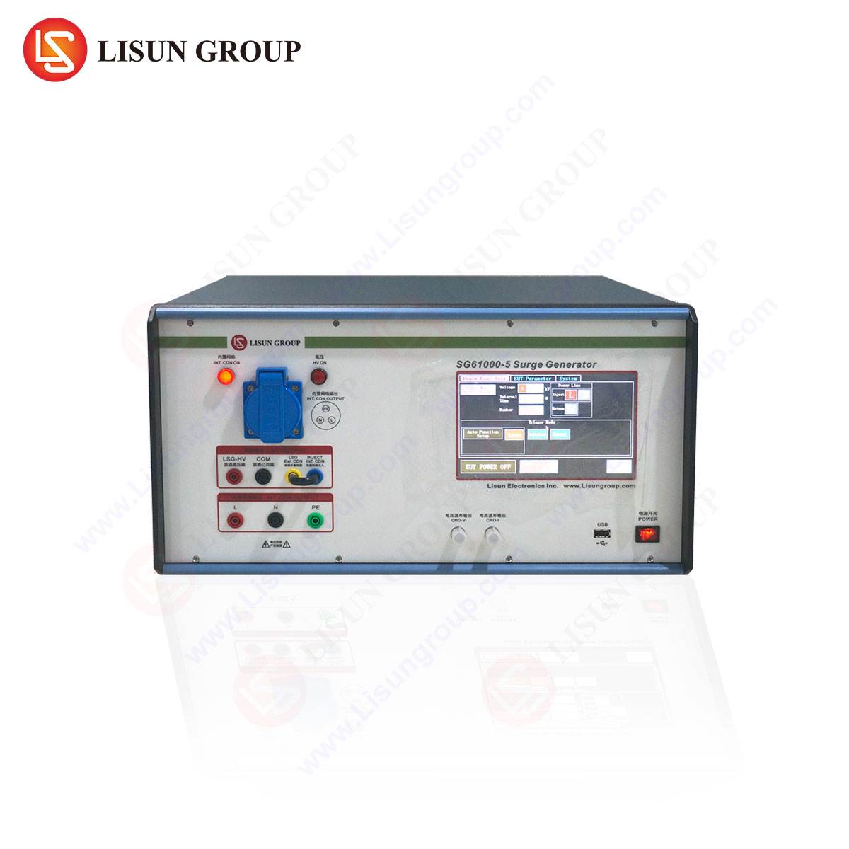
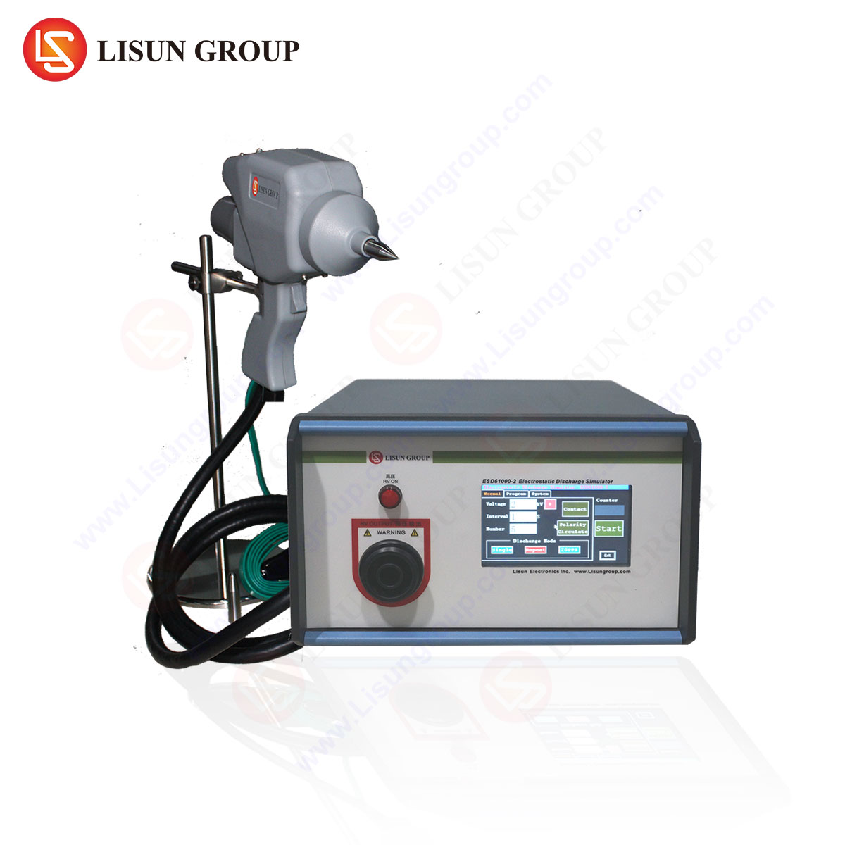
The LISUN ESD61000-2 ESD Simulator for Comprehensive System Testing
For rigorous and repeatable system-level ESD immunity testing, the LISUN ESD61000-2 ESD Simulator represents a state-of-the-art solution fully compliant with IEC 61000-4-2, ISO 10605, and other related standards. This instrument is engineered to generate precise and consistent ESD pulses, enabling accurate assessment of a product’s resilience in its operational environment.
Testing Principles and Specifications:
The core of the ESD61000-2 is its ability to generate the standardized ESD waveform defined by IEC 61000-4-2. The key waveform parameters are a rise time of 0.7 to 1 nanosecond and a current pulse that decays to 50% of its peak value at 30 nanoseconds and to 10% at 60 nanoseconds. The simulator offers test voltages up to 30 kV, covering the full range required for both contact and air discharge testing. Its advanced design ensures minimal waveform ringing and overshoot, which is critical for obtaining reliable and reproducible test results. The unit features a digital display for real-time voltage monitoring, a countdown function for automated test sequences, and both single and repetitive discharge modes.
Industry Use Cases and Applications:
The versatility of the LISUN ESD61000-2 makes it applicable across a vast spectrum of industries.
- Automotive Industry & Rail Transit: Testing electronic control units (ECUs), infotainment systems, and sensors against the stringent ISO 10605 standard, which accounts for harsher ESD environments within a vehicle.
- Medical Devices: Validating the immunity of critical patient monitoring equipment, diagnostic instruments, and portable medical devices to ensure operational safety and data integrity.
- Household Appliances & Power Tools: Assessing the robustness of touch controls, display interfaces, and motor controllers against ESD from user interaction.
- Lighting Fixtures & Intelligent Equipment: Testing smart lighting systems and IoT devices where user interfaces and external communication ports are susceptible to ESD.
- Communication Transmission & Information Technology Equipment: Ensuring network switches, routers, and servers can withstand ESD events on data ports and chassis without service interruption.
Competitive Advantages:
The LISUN ESD61000-2 distinguishes itself through several key features. Its high voltage (HV) relay is rated for over 1,000,000 discharges, ensuring long-term reliability and minimal maintenance. The generator’s compact and ergonomic design facilitates ease of use during extended testing sessions. Furthermore, its robust construction and stable performance provide superior repeatability and correlation of test data, a critical factor for quality assurance laboratories and certification bodies. The inclusion of multiple discharge network modules (e.g., 150pF/330Ω for IEC, 150pF/2000Ω for automotive) in some configurations offers expanded testing capabilities.
Mitigation Strategies: A Multi-Layered Approach from Factory to Field
Effective ESD control is not a single action but a comprehensive, multi-layered program that spans the entire product lifecycle, from semiconductor fabrication to end-user application.
- ESD-Protected Areas (EPAs): Critical manufacturing, assembly, and repair areas must be designated as EPAs. These zones are equipped with conductive or dissipative work surfaces, grounded wrist straps, and floor mats to safely bleed away static charges. Ionizers are used to neutralize charges on insulating materials that cannot be grounded.
- Proper Grounding: All conductors, including personnel, equipment, and work surfaces, must be bonded to a common ground point. This equalizes potentials and prevents discharges.
- Protective Packaging: Sensitive components and assemblies are transported and stored in shielding bags, conductive foam, or containers that provide a Faraday cage effect, isolating the contents from external electrostatic fields.
- Circuit Design and Board Layout: On-board protection is the last line of defense. This includes the strategic use of transient voltage suppression (TVS) diodes, polymer-based suppressors, ferrite beads, and spark gaps. Careful board layout to minimize loop areas and the proper routing of traces near I/O connectors are also essential design practices, particularly for high-speed communication transmission equipment and sensitive instrumentation.
- Awareness and Training: A successful ESD program is dependent on a well-trained workforce. Personnel must understand the sources and dangers of ESD and be rigorously trained in the correct handling procedures.
Frequently Asked Questions (FAQ)
Q1: What is the primary difference between the IEC 61000-4-2 and ISO 10605 standards, and why does it matter for automotive testing?
The fundamental difference lies in the discharge network. IEC 61000-4-2 uses a 150pF capacitor and a 330Ω discharge resistor, simulating a discharge from a person standing on a floor. ISO 10605, tailored for the automotive environment, often uses a 150pF/330Ω network for direct discharges but also specifies a 330pF/2kΩ network to simulate a person seated in a vehicle (with higher capacitance due to the seat) discharging through higher-resistance paths like clothing. The LISUN ESD61000-2 can be configured with these different networks, making it suitable for testing both consumer and automotive electronics.
Q2: Why is the rise time of the ESD pulse so critical in system-level testing?
The extremely fast rise time (sub-nanosecond) of an ESD pulse means it contains very high-frequency spectral components. These high-frequency energies can easily couple parasitically into nearby printed circuit board traces, acting as efficient antennas. This coupling can induce voltages large enough to upset or damage sensitive integrated circuits, even if the discharge point is physically distant. A simulator with a poorly controlled rise time will not accurately replicate this real-world coupling effect, leading to non-representative test results.
Q3: Our products are fully enclosed in plastic housings with no exposed metal. Is system-level ESD testing still necessary?
Absolutely. While a plastic housing prevents direct contact discharge, it does not prevent an air discharge from occurring. A strong electrostatic field can arc through small gaps, ventilation holes, or even the plastic material itself if the field strength is sufficient. Furthermore, the electromagnetic pulse (EMP) generated by an ESD event can radiate through the housing and couple into internal circuitry. System-level testing is essential to verify that the design is immune to these indirect effects.
Q4: Can the LISUN ESD61000-2 be used for testing components, not just finished systems?
No, the ESD61000-2 is designed specifically for system-level testing per IEC 61000-4-2 and related standards. Its discharge network and waveform parameters are different from those required for component-level testing (HBM, MM, CDM). Component-level testing requires specialized, highly accurate testers like the LISUN ESD-883D (for HBM/MM) or ESD-CDM testers, which are designed to handle individual semiconductor devices in a controlled socketed environment with precise waveform verification. Using a system-level gun on a discrete component would not yield valid or reliable results and would likely destroy the component.