


Fundamental Principles of the Charged Device Model in Electrostatic Discharge
Electrostatic Discharge (ESD) represents a significant threat to the reliability and longevity of electronic components and systems. While the Human Body Model (HBM) has historically been a primary focus for simulating ESD events from a human operator, the Charged Device Model (CDM) addresses a fundamentally different and increasingly critical failure mechanism. The CDM ESD test simulates the rapid discharge of static charge that has accumulated on the device itself. This occurs when a charged component, such as an integrated circuit (IC) on a conveyor belt or a printed circuit board (PCB) during handling, comes into contact with a grounded surface or a conductor at a lower potential. The discharge event in CDM is characterized by an extremely fast rise time, typically in the range of 200 to 500 picoseconds, and a short total duration of less than 5 nanoseconds. This results in a current pulse with very high peak current, often exceeding 10 Amperes, despite the relatively low energy involved compared to HBM.
The physics of a CDM event are governed by the capacitance of the device and the voltage to which it has been charged. The discharge current, I_CDM, can be approximated by the equation I_CDM ≈ C_Device * dV/dt, where C_Device is the capacitance of the device under test (DUT) and dV/dt is the rate of voltage change. The exceptionally high dV/dt is what makes CDM particularly destructive. This rapid current transient can cause catastrophic failure modes such as gate oxide breakdown in CMOS transistors, melting of metal interconnects, and junction damage. These failures are often latent, meaning the component may pass initial functional tests but suffer from reduced operational lifespan and premature failure in the field. Consequently, CDM testing is not merely a complementary check but an essential qualification requirement for modern electronics across all industries.
Comparative Analysis of ESD Standards: ANSI/ESDA/JEDEC JS-002
The standardization of CDM testing methodologies is critical for ensuring consistent, reproducible, and meaningful results across different laboratories and manufacturers. The dominant standard governing this area is ANSI/ESDA/JEDEC JS-002, titled “Charged Device Model (CDM) – Component Level.” This standard supersedes earlier versions and provides a unified framework that has been jointly developed by the ESD Association (ESDA) and the Joint Electron Device Engineering Council (JEDEC). The JS-002 standard meticulously defines all aspects of the test procedure, including the calibration and qualification of the test system, the setup of the Field-Induced Charging method, the waveform verification requirements, and the pass/fail criteria.
A key element defined by JS-002 is the use of a specific calibration module with a known capacitance (typically 4pF or 6.8pF) to verify that the test system generates a current waveform that falls within the specified limits for peak current, rise time, and full width at half maximum. The standard outlines two discharge networks, one for non-socketed testing (Direct Contact) and one for socketed testing, each with defined resistor and inductor values to accurately simulate the real-world discharge path. Compliance with JS-002 is a non-negotiable prerequisite for component suppliers in industries such as Automotive, Medical Devices, and Aerospace, where product reliability is paramount. Adherence to this standard ensures that components can withstand the rigors of automated manufacturing, handling, and transportation processes without succumbing to CDM-type ESD damage.
The Field-Induced Charging Methodology in CDM Testing
The modern and standardized approach to CDM testing employs the Field-Induced Charging method. This technique ensures a consistent and repeatable way to charge the DUT, which is crucial for obtaining reliable data. In this setup, the DUT is placed on an insulating surface, typically a thin FR4 or ceramic plate, which is situated on a grounded field plate (Ground Plane). A charging probe, connected to a high-voltage source, is then positioned above the DUT. When a high voltage is applied to this charging probe, an electric field is established, inducing an opposite charge on the conductive parts of the DUT. The DUT itself becomes electrically floating due to the insulating layer.
The charging process is essentially creating a capacitor, with the charging probe as one plate and the DUT as the other. The amount of charge on the DUT is proportional to the applied voltage and the capacitance of this arrangement. Once the DUT is charged to the desired test voltage (e.g., ±500V, ±1kV), the high-voltage source is disconnected, and the charging probe is retracted. The actual discharge is initiated by bringing a grounded pogo pin-type discharge head into contact with a pin of the DUT. The stored charge on the device then discharges violently through this low-inductance path to ground, replicating a real-world CDM event. This method is superior to the older Direct Charging method as it prevents pre-stressing of the device and provides a more realistic simulation of how a device becomes charged in a production environment.
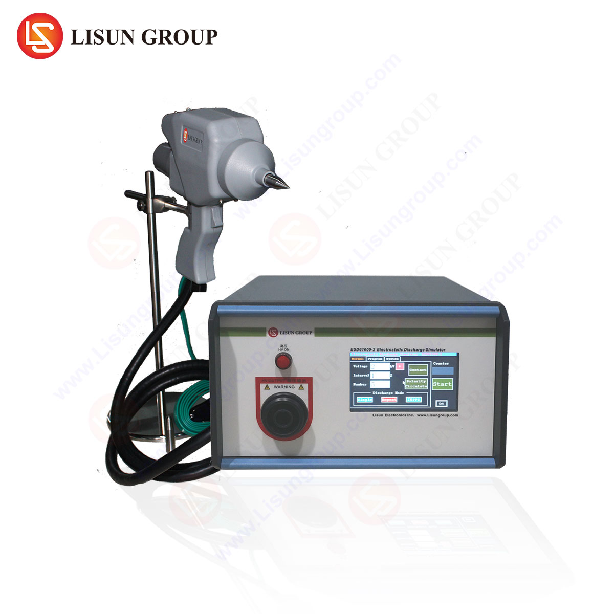
Operational Mechanics of the LISUN ESD61000-2 ESD Simulator
The LISUN ESD61000-2 Electrostatic Discharge Simulator is a precision instrument engineered to perform CDM testing in strict compliance with the ANSI/ESDA/JEDEC JS-002 standard. Its design integrates the core principles of field-induced charging into a reliable and user-friendly system. The apparatus consists of several key subsystems: a high-voltage DC power supply, a charging probe with a pneumatic or motorized lift mechanism, a grounded field plate, a high-speed discharge head with a low-inductance pogo pin, and a current waveform verification fixture.
The operational sequence is automated and controlled via a software interface. The test operator selects the desired test voltage level, which the high-voltage supply delivers to the charging probe. The probe descends, establishing the electric field to charge the DUT. After a predefined charging time, the probe retracts, and the discharge head is rapidly engaged with the specified pin on the DUT. The resultant discharge current waveform is captured using a high-bandwidth oscilloscope (typically >1 GHz) connected via a current transducer. The ESD61000-2 is designed with minimal parasitic inductance in the discharge path to ensure the generated waveform meets the stringent rise time and peak current requirements of the JS-002 standard. Its robust construction ensures long-term mechanical stability, which is critical for maintaining calibration and repeatability over thousands of test cycles.
Technical Specifications and Calibration of a JS-002 Compliant System
A CDM test system like the LISUN ESD61000-2 is characterized by a set of precise technical specifications that define its performance envelope. These specifications are directly derived from the requirements of the JS-002 standard.
Key Specifications of the LISUN ESD61000-2:
- Test Voltage Range: 125 V to 1,250 V (Positive and Negative Polarities)
- Charging Method: Field-Induced, in accordance with JS-002
- Discharge Network: Integrated, switchable for different standard requirements
- Voltage Rise/Settle Time: < 1 second to the target voltage
- Discharge Head Inductance: Minimized to < 10 nH to ensure waveform fidelity
- Waveform Verification: Supports calibration with 4pF and 6.8pF modules as per JS-002
- Control Interface: Touchscreen with PC software for test plan management and data logging
Calibration is a cornerstone of reliable CDM testing. The system must be periodically verified using a standard calibration module, such as a 4pF ceramic capacitor with a defined geometry. The verification process involves placing the module on the test platform, charging it to a specific voltage (e.g., 500V), and discharging it through the system. The captured current waveform must conform to the parameters specified in the JS-002 standard. The table below outlines the target waveform parameters for a 500V discharge using a 4pF calibration module:
| Waveform Parameter | JS-002 Requirement (for 4pF, 500V) | Typical LISUN ESD61000-2 Performance |
|---|---|---|
| First Peak Current (Ip1) | 7.5 A to 10.5 A | 9.0 A ± 0.5 A |
| Rise Time (tr) | 175 ps to 350 ps | 250 ps ± 50 ps |
| Full Width at Half Max (FWHM) | 350 ps to 650 ps | 500 ps ± 100 ps |
| Second Peak Current (Ip2) | 5.0 A to 7.5 A | 6.5 A ± 0.5 A |
Industry-Specific Applications for CDM ESD Qualification
The necessity for CDM ESD immunity spans a vast array of industries, driven by the ubiquity of sensitive electronics and the automation of manufacturing processes.
- Automotive Industry: Electronic Control Units (ECUs), sensors, and infotainment systems are handled extensively on automated lines. A CDM event during assembly could cause a latent failure in a braking or airbag control module, with severe safety implications. CDM testing is mandated by most automotive quality standards (e.g., AEC-Q100).
- Medical Devices: Implantable devices like pacemakers and neurostimulators, as well as critical diagnostic equipment like MRI machines and patient monitors, contain highly sensitive analog and digital ICs. A CDM failure could lead to inaccurate readings or device malfunction, directly impacting patient safety.
- Communication Transmission & Information Technology Equipment: Network switches, routers, and base station components are populated with high-pin-count, fine-geometry ASICs and FPGAs. These devices are highly susceptible to gate oxide damage from CDM, which can lead to systemic failures in communication infrastructure.
- Industrial Equipment & Power Tools: Variable-frequency drives, programmable logic controllers (PLCs), and smart motor controllers operate in harsh electrical environments. CDM robustness ensures these components can survive the manufacturing and assembly process before being subjected to in-circuit electrical stresses.
- Aerospace, Rail Transit, and Spacecraft: The extreme cost of failure and the inability to perform repairs in situ make ESD qualification non-negotiable. Every electronic component, from those used in flight control systems to passenger entertainment modules in trains, must be rigorously tested against CDM events to ensure decades of reliable operation.
- Household Appliances and Lighting Fixtures: The proliferation of smart, connected appliances with sophisticated control boards means that even a simple washing machine or LED driver contains microcontrollers and power management ICs that require CDM protection to achieve acceptable field return rates.
Analysis of Common CDM Failure Signatures in Electronic Components
CDM stress induces failure mechanisms that are distinct from those caused by HBM or Machine Model (MM) ESD. The ultra-fast, high-current pulse leads to localized, intense heating and immense electric fields over very small areas.
- Gate Oxide Breakdown: This is the most common CDM failure mode in CMOS technologies. The extremely high voltage gradient across the thin gate oxide (dV/dt) during the discharge causes a rupture, creating a short or a leaky path between the gate and the channel. This failure is often catastrophic and permanent.
- Junction Spiking and Melting: The high current density through source/drain junctions or substrate contacts can cause localized heating that melts the silicon and metal silicides, forming a short circuit.
- Metal Interconnect Damage: The sudden current surge can electromigrate or vaporize fine metal traces, especially at vias and contacts where current density is highest, leading to an open circuit.
- Latch-Up Triggering: The CDM transient can induce substrate currents that trigger parasitic silicon-controlled rectifier (SCR) structures, leading to latch-up. While potentially reversible, latch-up can cause functional failure and, if sustained, thermal destruction.
Failure analysis techniques such as Emission Microscopy (EMMI), Optical Beam Induced Resistance Change (OBIRCH), and focused ion beam (FIB) cross-sectioning are routinely used to pinpoint these microscopic CDM failure signatures.
Integrating CDM Robustness into Product Design and Manufacturing
Achieving CDM immunity is not solely a testing activity; it must be incorporated into the product lifecycle from design through production. At the Integrated Circuit (IC) design level, this involves the strategic placement of dedicated CDM protection circuits at every bond pad. These circuits are designed to clamp the voltage during a CDM event by providing an ultra-fast, low-impedance shunt path to either the power supply rail or ground. The design of these structures is a complex trade-off between protection level, speed, and parasitic effects that can impact circuit performance.
At the board and system level, manufacturing processes must be controlled to minimize charge generation and accumulation. This includes the use of conductive totes, ionizers to neutralize static charge, and grounding straps for personnel and workstations. Implementing a comprehensive Electrostatic Protected Area (EPA) is a foundational practice. However, the first and most critical line of defense remains the inherent CDM robustness designed into the components themselves, which is why qualification with a system like the LISUN ESD61000-2 is so vital.
Frequently Asked Questions (FAQ)
Q1: What is the primary functional difference between the LISUN ESD61000-2 and an HBM ESD simulator?
The fundamental difference lies in the discharge network and the test methodology. An HBM simulator uses a 100pF capacitor and a 1.5kΩ resistor to simulate a discharge from a human body, resulting in a slower, lower-current pulse with a rise time of ~10 nanoseconds. The LISUN ESD61000-2 uses a field-induced charging method with a direct, low-inductance discharge path to simulate a charged device discharging, producing a much faster (<1 ns) and higher-amplitude current pulse.
Q2: Why is waveform verification so critical in CDM testing, and how often should it be performed?
Waveform verification ensures the test system is generating a discharge that accurately replicates the real-world CDM event as defined by the JS-002 standard. Even small changes in parasitic inductance or resistance can alter the waveform, leading to non-compliant testing that either over-stresses (causing unnecessary yield loss) or under-stresses (allowing weak components to pass) the DUT. It is recommended to perform verification before starting a test series, after any maintenance, and at regular intervals as defined by the lab’s quality procedures (e.g., daily or weekly).
Q3: Can the LISUN ESD61000-2 be used to test assembled printed circuit boards (PCBs), or is it only for individual components?
While the JS-002 standard is defined at the component level, the field-induced CDM phenomenon also occurs at the board level. The LISUN ESD61000-2 can be adapted for board-level testing, though the test setup and pass/fail criteria may need to be defined by the user or based on other applicable standards, as the capacitance of a full PCB is significantly larger than that of a single component. The system’s flexibility allows for such specialized applications.
Q4: Our company manufactures household appliances. At what stage in our product development should we require CDM testing data from our component suppliers?
CDM qualification data should be a mandatory part of the component selection and qualification process, prior to finalizing your Bill of Materials (BOM). Requiring that all sensitive ICs (microcontrollers, drivers, sensors) are certified to a specific CDM withstand level (e.g., ±500V per JS-002) is a best practice for Design-for-Reliability (DfR). This proactive step is far more cost-effective than dealing with field failures and product recalls linked to ESD damage.
Q5: How does the system ensure consistent contact during the discharge event?
The LISUN ESD61000-2 employs a precision, spring-loaded pogo pin in the discharge head. This ensures a consistent, low-resistance, and low-inductance electrical contact with the device pin for every discharge. The force and travel of the pin are engineered to provide reliable contact without causing physical damage to the pin or package of the DUT.